Sic epitaxial wafer

Inactive Publication Date: 2019-05-16
SHOWA DENKO KK
View PDF1 Cites 5 Cited by
  • Summary
  • Abstract
  • Description
  • Claims
  • Application Information

AI Technical Summary

Benefits of technology

[0014]A SiC epitaxial wafer according to the present invention makes it poss

Problems solved by technology

In the SiC epitaxial wafer, basal plane dislocations (BPDs) are known as device killer-defects which cause critical defects on the SiC device.
In contrast, a part of the basal plane dislocations carried over in the epitaxial layer become device killer defects.
When forward curre

Method used


Image

  • Sic epitaxial wafer
  • Sic epitaxial wafer
  • Sic epitaxial wafer

Examples


example 1

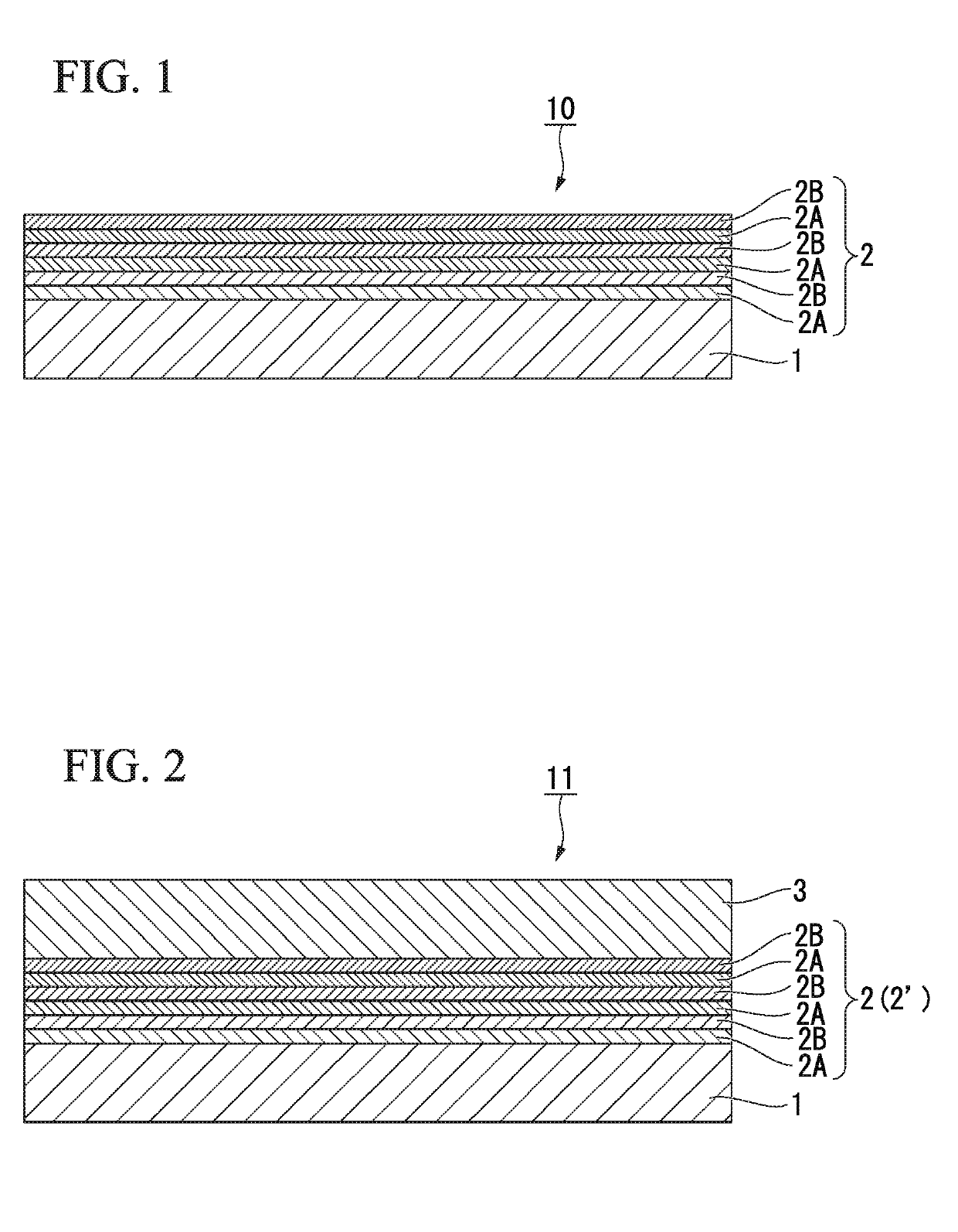
[0077]A SiC single crystal substrate having a diameter of 100 mm was prepared. The prepared SiC single crystal substrate is a 4H-type polytype and the main face thereof has a Si face having an offset angle of 4° in the direction from the (0001) face.

[0078]Then, the SiC single crystal substrate is introduced into a reactor, and a raw material gas (composed of trichlorosilane, propane, and hydrogen chloride) is introduced at a growth temperature of 1600° C. to conduct the epitaxial growth. Nitrogen was used as a doping gas. At the time, the dopant incorporation efficiency was changed by changing the ratio C / Si at the growth in a range from 0.8 to 1.0 over time.

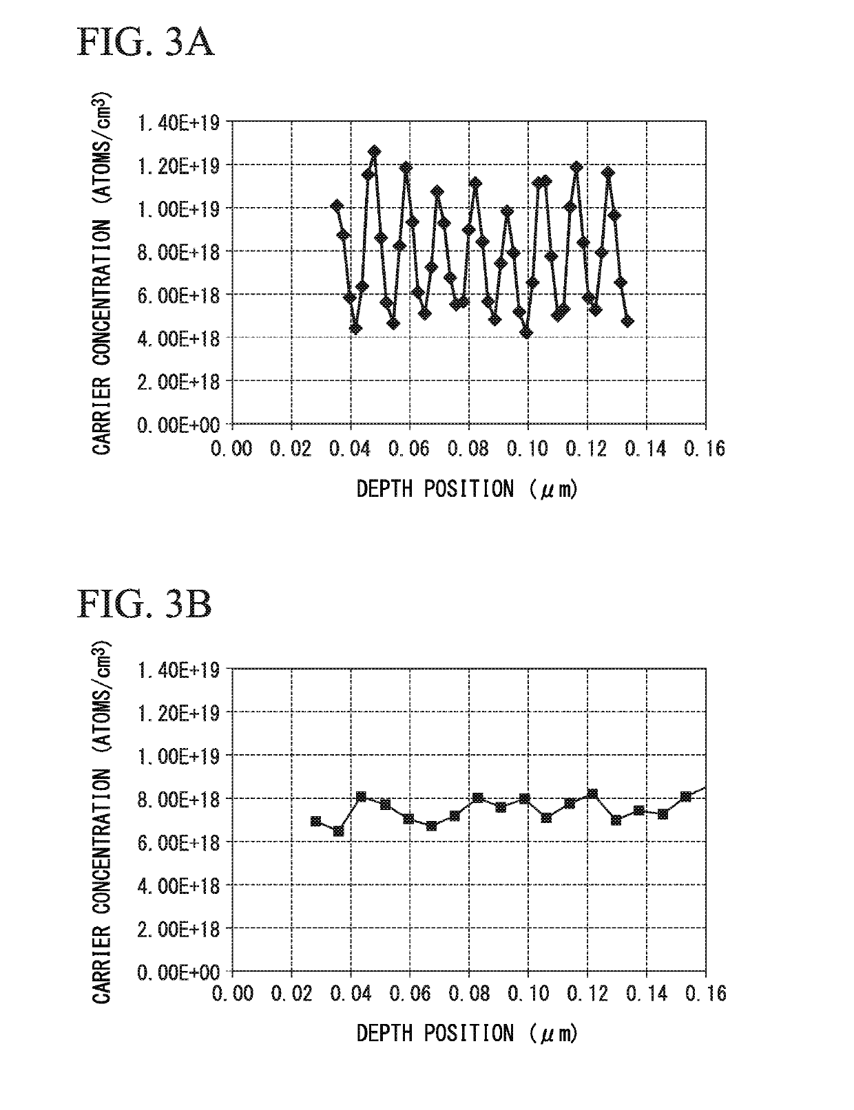
[0079]Then, the carrier concentration in a thickness direction of the obtained epitaxial layer was measured using secondary ion mass spectrometer (SIMS). The carrier concentration in a thickness direction was measured using SIMS while shaving the epitaxial layer in a depth direction. The results thereof are shown in FIG. 3A.

[00...


PUM


Abstract

An SiC epitaxial wafer according to the present invention includes: an SiC single crystal substrate; and a carrier concentration variation layer disposed on one face side of the SiC single crystal substrate, wherein the carrier concentration variation layer includes: high concentration layers in which carrier concentrations thereof are higher than carrier concentrations of adjacent layers; and low concentration layers in which carrier concentrations are lower than in adjacent layers, and the high concentration layers and the low concentration layers are laminated alternately.

Description

TECHNICAL FIELD[0001]The present invention relates to a SiC epitaxial wafer.BACKGROUND OF THE INVENTION[0002]Silicon carbide (SiC) has: a breakdown electric field larger than that of silicon (Si) by one order of magnitude; a band gap three times as larger as that of Si; and a thermal conductivity approximately three times as high as that of Si. Accordingly, silicon carbide (SiC) has been expected to be applied to power device, high-frequency device, high-temperature operational device, or the like.[0003]It is required to establish a high-quality SiC epitaxial wafer and a high-quality epitaxial growth-technique so as to promote the practical realization of the Sic device.[0004]A SiC device is formed on a SiC epitaxial wafer including: a SiC substrate; and an epitaxial layer laminated on the substrate. The SiC substrate is obtained by processing SiC bulk single crystals grown by a sublimation-recrystallization method or the like. The epitaxial layer is formed by a chemical vapor depos...

Claims


Application Information

Patent Timeline
IPC IPC(8): H01L29/16H01L29/06H01L21/02H01L29/04
CPCH01L29/1608H01L29/06H01L21/02529H01L21/0262H01L21/02576H01L21/02579H01L21/02433H01L21/02634H01L29/045H01L21/02378H01L21/02447
Inventor ISHIBASHI, NAOTOFUKADA, KEISUKE
Owner SHOWA DENKO KK
Why Eureka
Try Eureka