Method of manufacturing semiconductor light emitting device

a technology of light emitting devices and semiconductors, which is applied in the direction of semiconductor/solid-state device manufacturing, semiconductor devices, electrical devices, etc., can solve the problems of increasing bulk resistance, and achieve the effect of increasing the light extraction efficiency of semiconductor light emitting devices

Active Publication Date: 2019-09-12
NIKKISO COMPANY
View PDF4 Cites 0 Cited by
  • Summary
  • Abstract
  • Description
  • Claims
  • Application Information

AI Technical Summary

Benefits of technology

[0005]In this background, one illustrative purpose of the present invention is to provide a...

Problems solved by technology

It is known that dry-etching of the n-type clad layer of an AlGaN-based semiconductor material induces nitrogen d...

Method used


Image

  • Method of manufacturing semiconductor light emitting device
  • Method of manufacturing semiconductor light emitting device
  • Method of manufacturing semiconductor light emitting device

Examples


Embodiment Construction

[0020]The invention will now be described by reference to the preferred embodiments. This does not intend to limit the scope of the present invention, but to exemplify the invention.

[0021]A detailed description will be given of embodiments to practice the present invention with reference to the drawings. Like numerals are used in the description to denote like elements and a duplicate description is omitted as appropriate. To facilitate the understanding, the relative dimensions of the constituting elements in the drawings do not necessarily mirror the relative dimensions in the actual apparatus.

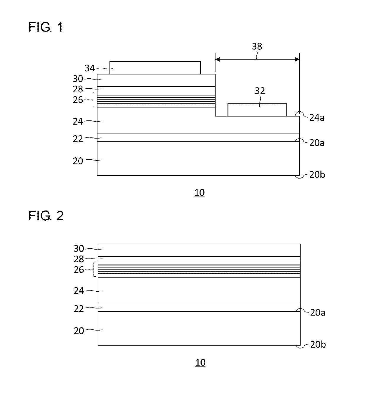
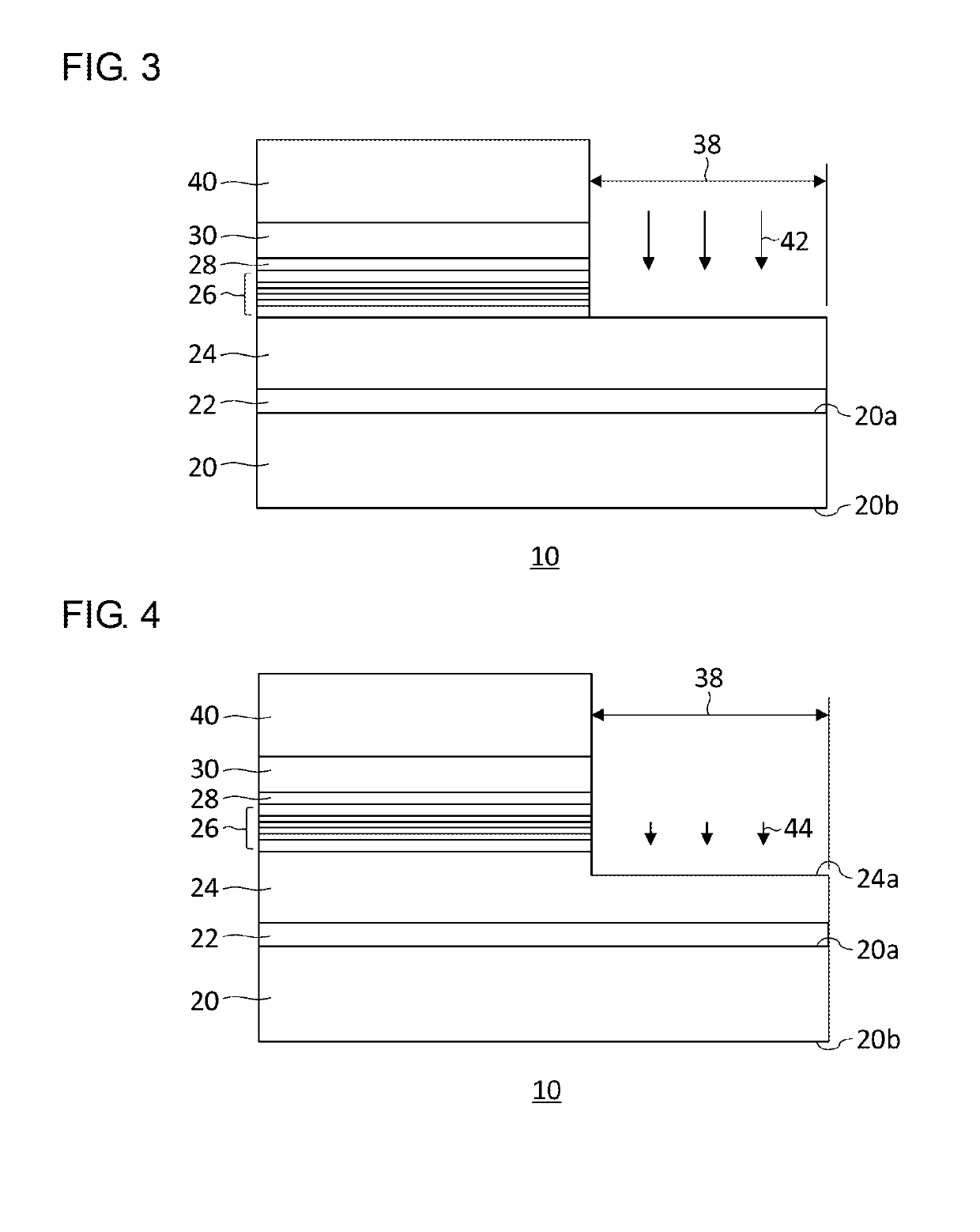
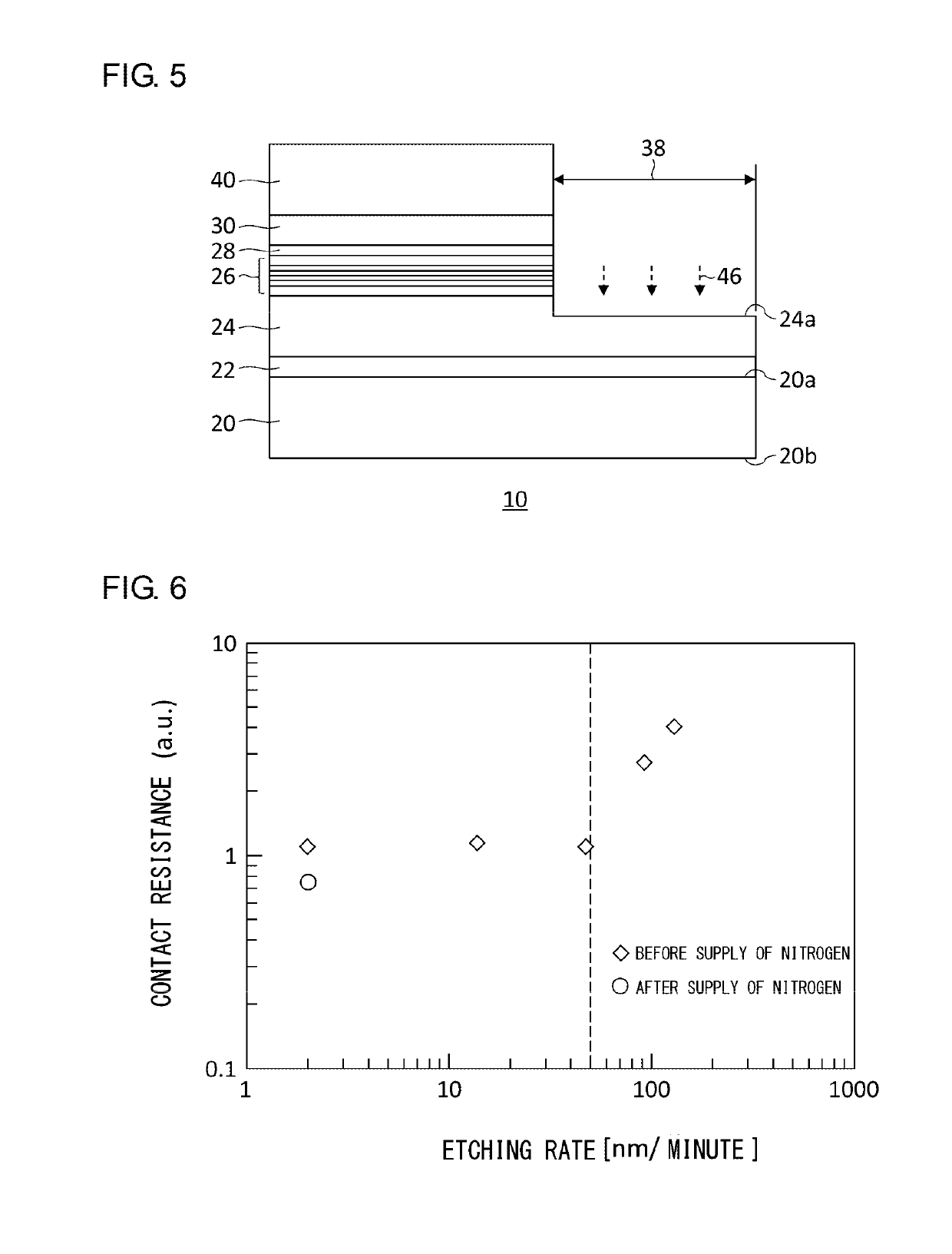
[0022]FIG. 1 is a cross-sectional view schematically showing a configuration of a semiconductor light emitting device 10 according to the embodiment. The semiconductor light emitting device 10 is a light emitting diode (LED) chip configured to emit “deep ultraviolet light” having a central wavelength λ of about 360 nm or lower. To output deep ultraviolet light having such a wavelength, the s...


PUM


Abstract

A method of manufacturing a semiconductor light emitting device includes: forming an active layer of an aluminum gallium nitride (AlGaN)-based semiconductor material on an n-type clad layer of an n-type AlGaN-based semiconductor material; forming a p-type semiconductor layer on the active layer; dry-etching portions of the p-type semiconductor layer, the active layer, and the n-type clad layer so as to expose a partial region of the n-type clad layer; causing nitrogen atoms (N) to react with the partial region of the n-type clad layer exposed; and forming an n-side electrode on the partial region of the n-type clad layer that the nitrogen atoms are caused to react with.

Description

RELATED APPLICATION[0001]Priority is claimed to Japanese Patent Application No. 2016-228137, filed on Nov. 24, 2016, the entire content of which is incorporated herein by reference.BACKGROUND OF THE INVENTION1. Field of the Invention[0002]The present invention relates to a method of manufacturing semiconductor light emitting devices.2. Description of the Related Art[0003]Nowadays, semiconductor light emitting devices such as light emitting diodes and laser diodes that emit blue light have been in practical use. Development of light emitting devices that output deep ultraviolet light having a shorter wavelength has also been pursued. Deep ultraviolet light has sterilization capability. Semiconductor light emitting devices capable of outputting deep ultraviolet light have therefore attracted attention as a mercury free sterilization light source in medical and food processing fields. A light emitting device for emitting deep ultraviolet light includes an aluminum gallium nitride (AlGa...

Claims


Application Information

Patent Timeline
IPC IPC(8): H01L33/00H01L33/32H01L33/14H01L33/36
CPCH01L33/32H01L33/007H01L2933/0016H01L33/145H01L33/36H01L21/28H01L21/30621H01L21/3065
Inventor IGARASHI, KAZUSHIGENIWA, NORITAKAINAZU, TETSUHIKO
Owner NIKKISO COMPANY
Why Eureka
Try Eureka