Measurement Models Of Nanowire Semiconductor Structures Based On Re-Useable Sub-Structures

a semiconductor structure and measurement model technology, applied in semiconductor/solid-state device testing/measurement, instruments, computer-aided design, etc., can solve the problems of nanowire devices being particularly difficult to characterize, characterization difficulty, and characterization difficulty, so as to reduce the time to useful measurement results, less error prone, and more accurate

Active Publication Date: 2019-09-19
KLA TENCOR TECH CORP
View PDF2 Cites 4 Cited by
  • Summary
  • Abstract
  • Description
  • Claims
  • Application Information

AI Technical Summary

Benefits of technology

[0016]Methods and systems for generating measurement models of nanowire based semiconductor structures based on re-useable, parametric models are presented herein. Metrology systems employing these models are configured to measure structural and material characteristics (e.g., material composition, dimensional characteristics of structures and films, etc.) associated with nanowire semiconductor fabrication processes. The re-useable, parametric models of nanowire based semiconductor structures enable measurement model generation that is substantially simpler, less error prone, and more accurate. As a result, time to useful measurement results is significantly reduced, particularly when modelling complex, nanowire based structures. The re-useable, parametric models of nanowire based semiconductor structures are useful for generating measurement models for both optical metrology and x-ray metrology, e.g., soft x-ray metrology and hard x-ray metrology.
[0017]In one aspect, a model building tool includes re-useable, parametric models of complex device sub-structures useable as building blocks in a model of a complex nanowire based semiconductor device. This makes the model building process more intuitive and less error-prone. Furthermore, because the re-useable, parametric sub-structure models are optimized for nanowire based semiconductor structures and measurement applications, the resulting discretized measur

Problems solved by technology

As devices (e.g., logic and memory devices) move toward smaller nanometer-scale dimensions, characterization becomes more difficult.
Devices incorporating complex three-dimensional geometry and materials with diverse physical properties contribute to characterization difficulty.
Nanowire devices are particularly difficult to characterize, particularly with optical metrology.
Although models constructed from primitive structural building blocks offer a wide range of modeling flexibility and user control, the model building process becomes very complex and error prone when modeling nanowire based semiconductor structures.
Accomplishing this is not an easy task, and users spend significant amounts of time ensuring that their models are correct.
In many cases, users do not realize their models are inconsistent and incorrect because it is difficult to comprehend how all of the primitive structural building blocks change shape and location in parameter space.
Specifically, it is very difficult to determine if models that are structurally consistent for a given set of parameter values remain structurally consistent for another set of parameter values.
This makes model-building very complex and prone to user errors.
Furthermore, model complexity makes it difficult for one user to understand models built by another.
The user needs to be able to understand the intent of the original model owner and this becomes increasingly challenging as the number of primitive structural building blocks, constraints, and independent parameters increases.
Consequently, transferring ownership of models (e.g., from applications engineers to process engineers) is a time consuming, difficult process.
In many cases, the complexity of the models leads to frustration amongst colleagues, and in some cases, prevents the transfer process from ever being fully completed.
Unfortunately, existing primitive structural

Method used


Image

  • Measurement Models Of Nanowire Semiconductor Structures Based On Re-Useable Sub-Structures
  • Measurement Models Of Nanowire Semiconductor Structures Based On Re-Useable Sub-Structures
  • Measurement Models Of Nanowire Semiconductor Structures Based On Re-Useable Sub-Structures

Examples


Embodiment Construction

[0053]Reference will now be made in detail to background examples and some embodiments of the invention, examples of which are illustrated in the accompanying drawings.

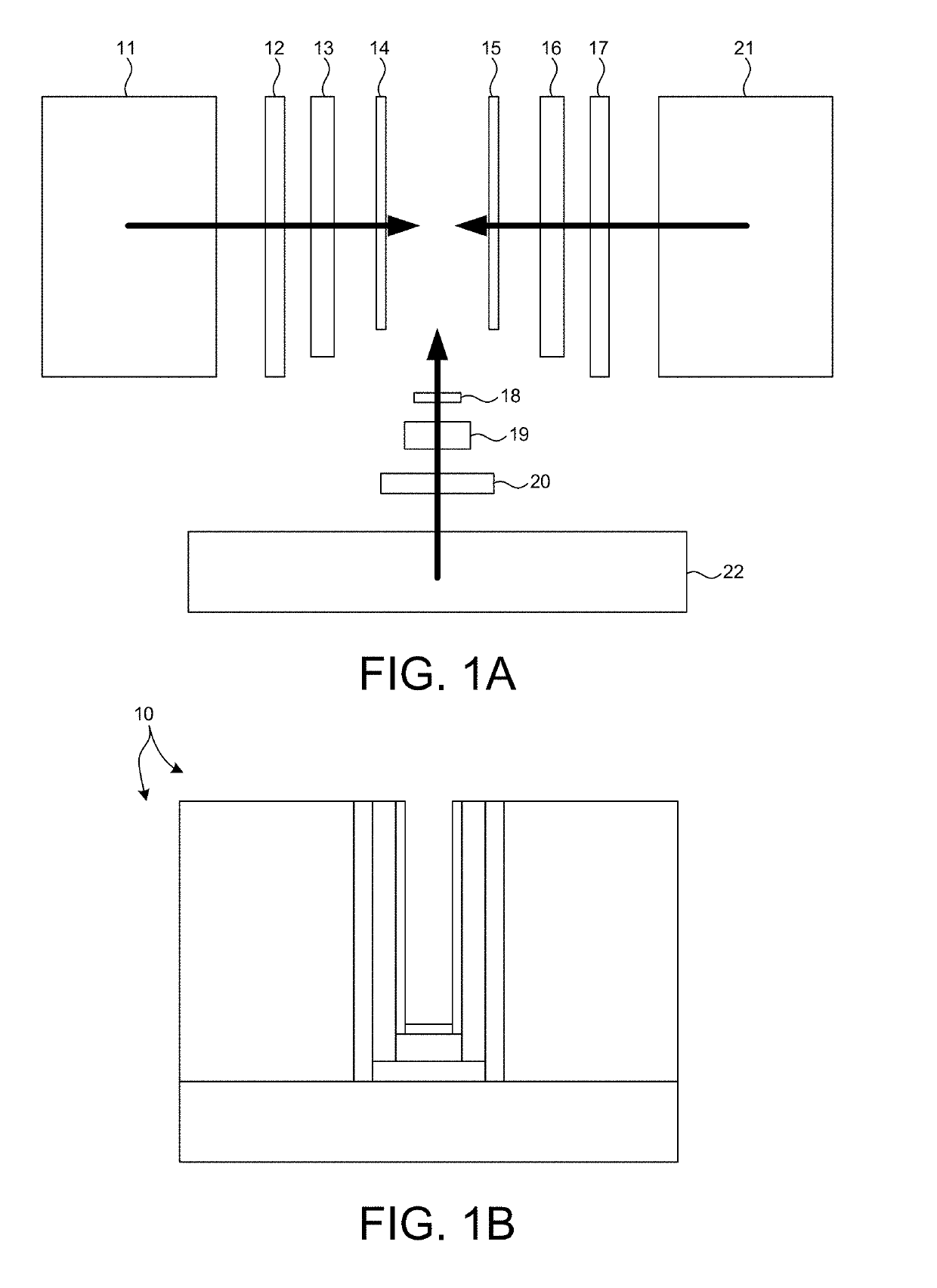
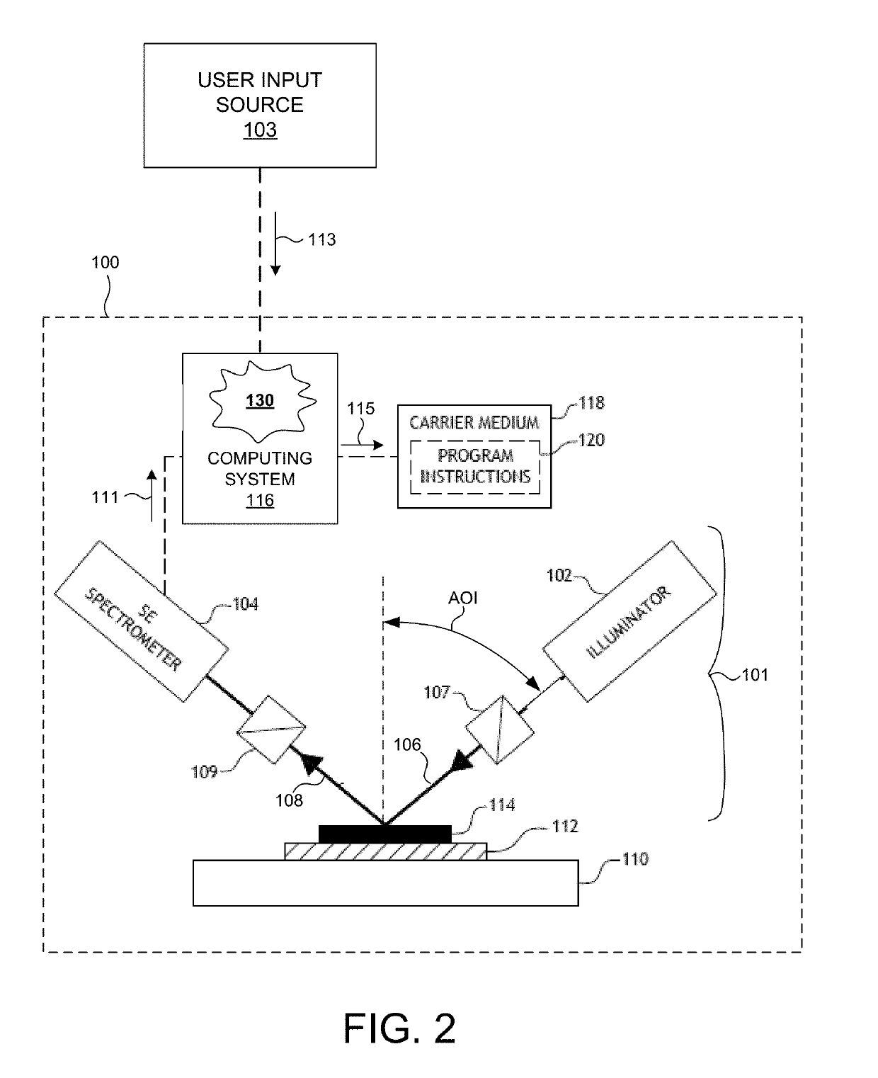
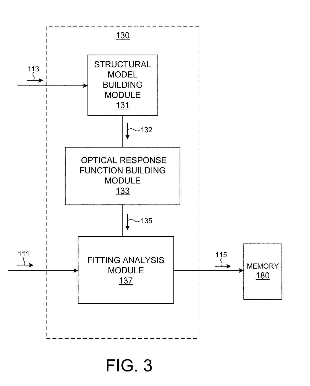
[0054]Scatterometry based metrology for critical dimensions (CDs), thin film thicknesses, optical properties and compositions, overlay, lithography focus / dose, etc., typically requires a geometric model of the underlying structure to be measured. This measurement model includes the physical dimensions, material properties, and parameterization of the structure.

[0055]Methods and systems for generating measurement models of nanowire based semiconductor structures based on re-useable, parametric models are presented herein. Metrology systems employing these models are configured to measure structural and material characteristics (e.g., material composition, dimensional characteristics of structures and films, etc.) associated with nanowire semiconductor fabrication processes. The re-useable, parametric models of nanowire...


PUM


Abstract

Methods and systems for generating measurement models of nanowire based semiconductor structures based on re-useable, parametric models are presented herein. Metrology systems employing these models are configured to measure structural and material characteristics (e.g., material composition, dimensional characteristics of structures and films, etc.) associated with nanowire semiconductor fabrication processes. The re-useable, parametric models of nanowire based semiconductor structures enable measurement model generation that is substantially simpler, less error prone, and more accurate. As a result, time to useful measurement results is significantly reduced, particularly when modelling complex, nanowire based structures. The re-useable, parametric models of nanowire based semiconductor structures are useful for generating measurement models for both optical metrology and x-ray metrology, including soft x-ray metrology and hard x-ray metrology.

Description

CROSS REFERENCE TO RELATED APPLICATION[0001]The present application for patent claims priority under 35 U.S.C. § 119 from U.S. provisional patent application Ser. No. 62 / 643,322, entitled “Methods And Tools For Generating Semiconductor Device Models With Nanowire Sub Structures,” filed Mar. 15, 2018, the subject matter of which is incorporated herein by reference in its entirety.TECHNICAL FIELD[0002]The described embodiments relate to metrology systems and methods, and more particularly to methods and systems for improved measurement accuracy.BACKGROUND INFORMATION[0003]Semiconductor devices such as logic and memory devices are typically fabricated by a sequence of processing steps applied to a specimen. The various features and multiple structural levels of the semiconductor devices are formed by these processing steps. For example, lithography among others is one semiconductor fabrication process that involves generating a pattern on a semiconductor wafer. Additional examples of s...

Claims


Application Information

Patent Timeline
IPC IPC(8): G06F17/50G01R31/309
CPCG06F17/5086G01R31/309B82Y30/00G01R31/311H01L21/67242H01L22/34H01L22/14H01L22/26G06F30/17
Inventor CHOUAIB, HOUSSAMKUZNETSOV, ALEXANDER
Owner KLA TENCOR TECH CORP
Why Eureka
Try Eureka