Mask blank, phase shift mask, method of manufacturing phase shift mask, and method of manufacturing semiconductor device

Inactive Publication Date: 2019-10-03
HOYA CORP
View PDF0 Cites 1 Cited by
  • Summary
  • Abstract
  • Description
  • Claims
  • Application Information

AI Technical Summary

Benefits of technology

[0092]The mask blank of this invention is a mask blank having a phase shift film on a transparent substrate, featured in that the phase shift film has a function to transmit an ArF exposure light at a transmittance of 10% or more, and a function to generate a phase difference of 150 degrees or more and 200 degrees or less, the phase shift film has a structure where a low transmitting layer and a high transmitting layer are stacked alternately in this order to form a total of six or more layers from a side of the transparent substrate, the low transmitting layer is made of a material containing silicon and nitrogen and having a nitrogen content of 50 atom % or more, the high transmitting layer is made of a material containing silicon and oxygen and having an oxygen content of 50 atom % or more, the low transmitting layer has a thickness greater than the thickness of the high transmitting layer, and the high transmitting layer has a thickness of 4 nm or less.
[0093]Further, the mask blank of this invention is a mask blank having a phase shift film on a transparent substrate, featured in that the phase shift film has a function to transmit an ArF exposure light at a transmittance of 10% or more, and a function to generate a phase difference of 150 degrees or more and 200 degrees or less, the phase shift film has a structure where a low transmitting layer and a high transmitting layer are stacked alternately in this order to form a total of six or more layers from a side of the transparent substrate, the low transmitting layer is made of a

Problems solved by technology

However, it has been discovered recently that a MoSi-based film has low resistance to exposure light of an ArF excimer laser (so-called ArF light fastness).
Particul

Method used


Image

  • Mask blank, phase shift mask, method of manufacturing phase shift mask, and method of manufacturing semiconductor device
  • Mask blank, phase shift mask, method of manufacturing phase shift mask, and method of manufacturing semiconductor device

Examples


example 1

[Manufacture of Mask Blank]

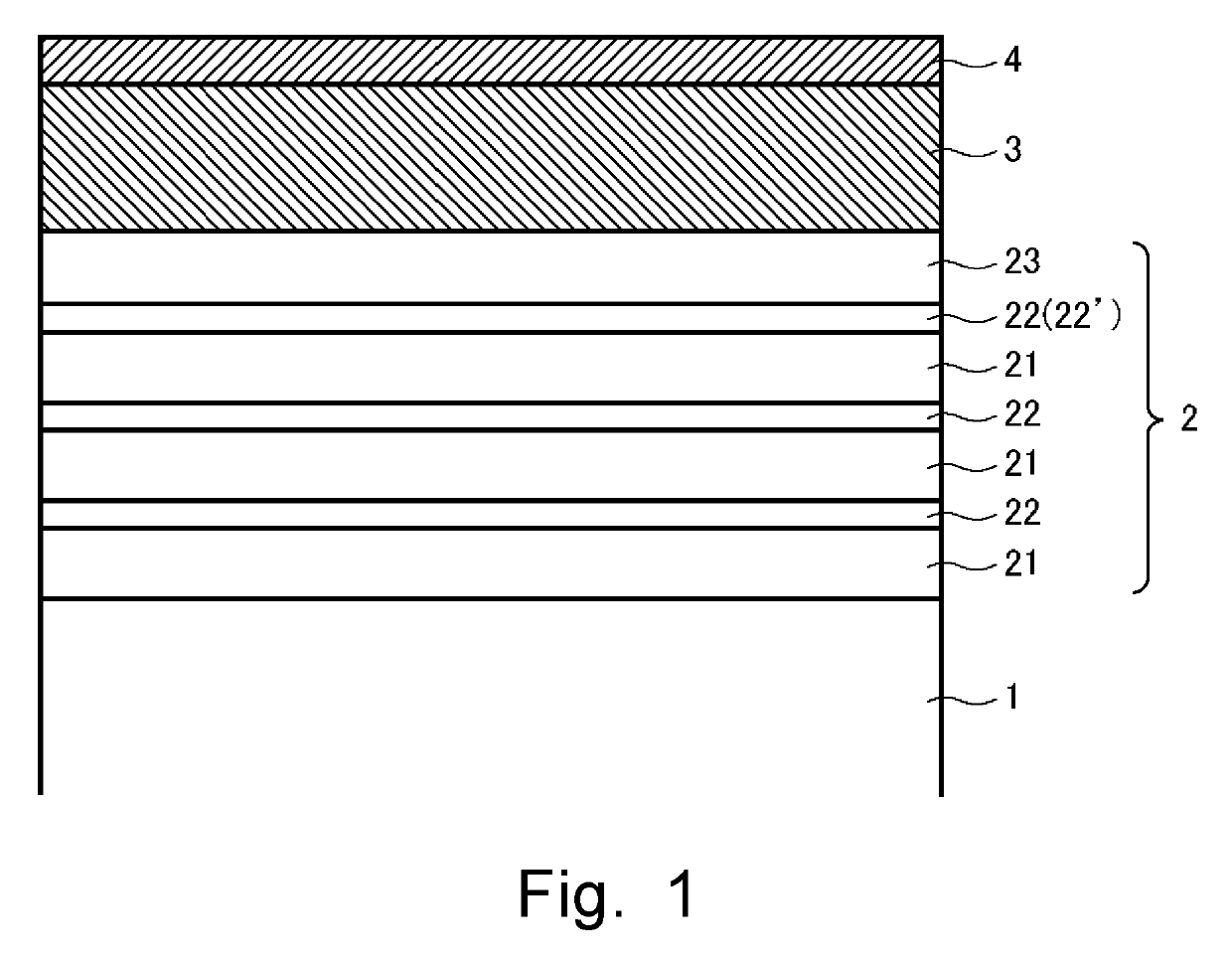
[0205]A transparent substrate 1 made of a synthetic quartz glass with a size of a main surface of about 152 mm×about 152 mm and a thickness of about 6.25 mm was prepared. An end surface and the main surface of the transparent substrate 1 were polished to a predetermined surface roughness, and thereafter subjected to predetermined cleaning treatment and drying treatment.

[0206]Next, the transparent substrate 1 was placed in a single-wafer RF sputtering apparatus, and by reactive sputtering (RF sputtering) using a silicon (Si) target with mixed gas of krypton (Kr), helium (He), and nitrogen (N2) (flow ratio Kr:He:N2=1:10:3, pressure=0.09 Pa) as sputtering gas and with 2.8 kW electric power of RF power source, a low transmitting layer 21 consisting of silicon and nitrogen (Si:N=44 atom %:56 atom %) was formed on the transparent substrate 1 at a thickness of 14.5 nm. On a main surface of another transparent substrate, only a low transmitting layer was formed un...


PUM


Abstract

A mask blank for a phase shift mask having a phase shift film on a transparent substrate. The phase shift film generates a phase difference of 150 degrees or more and 200 degrees or less and transmits exposure light of an ArF excimer laser at a transmittance of 10% or more. The film has a low transmitting layer and a high transmitting layer, stacked alternately to form a total of six or more layers from a side of the transparent substrate. The low transmitting layer is made of a material containing silicon and nitrogen and having a nitrogen content of 50 atom % or more. The high transmitting layer is made of a material containing silicon and oxygen and having an oxygen content of 50 atom % or more. The low transmitting layer has a thickness greater than that of the high transmitting layer, which has a thickness of 4 nm or less.

Description

TECHNICAL FIELD[0001]This invention relates to a mask blank, a phase shift mask manufactured using the mask blank, and a method of its manufacture. This invention further relates to a method of manufacturing a semiconductor device using the phase shift mask.BACKGROUND ART[0002]In a manufacturing process of a semiconductor device, photolithography is used to form a fine pattern. Multiple transfer masks are usually utilized in forming the fine pattern. In miniaturization of a semiconductor device pattern, it is necessary to shorten the wavelength of the exposure light source used in photolithography, in addition to miniaturization of a mask pattern formed on the transfer mask. In recent years, application of an ArF excimer laser (wavelength 193 nm) is increasing as an exposure light source in the manufacture of semiconductor devices.[0003]A type of a transfer mask is a half tone phase shift mask. The half tone phase shift mask has a light transmission portion for transmitting an expos...

Claims


Application Information

Patent Timeline
IPC IPC(8): G03F1/30G03F1/00G03F1/74H01L21/308
CPCH01L21/3081G03F1/74G03F1/0076G03F1/0061G03F1/30G03F1/32G03F7/2053G03F7/70025G03F7/70958H01L21/3065
Inventor HORIGOME, YASUTAKATANIGUCHI, KAZUTAKESHISHIDO, HIROAKI
Owner HOYA CORP
Why Eureka
Try Eureka