Epitaxy-Free Nanowire Cell Process for the Manufacture of Photovoltaics
a nanowire cell and photovoltaic technology, applied in the direction of electrical equipment, semiconductor/solid-state device manufacturing, semiconductor devices, etc., can solve the problems of economic inviability and limited economic scalability of high-efficiency solar cells, and achieve economic scalability and economic benefits
- Summary
- Abstract
- Description
- Claims
- Application Information
AI Technical Summary
Benefits of technology
Problems solved by technology
Method used
Image
Examples
exemplary embodiment 1
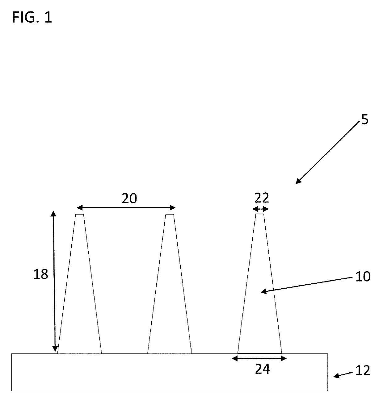
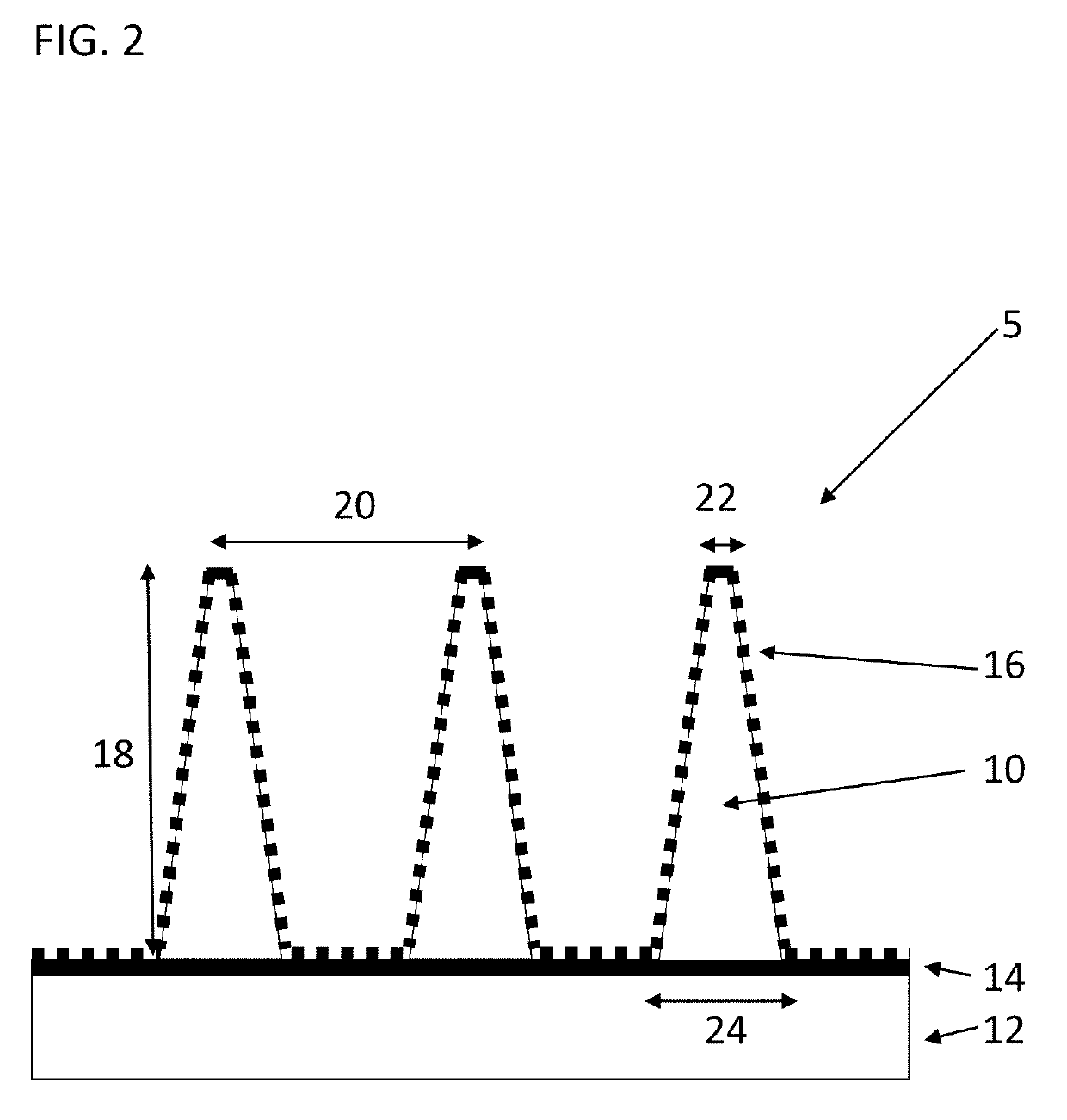
[0089]To test the efficiency of solar cells formed in accordance with embodiments, a GaAs heterojunction solar cell, as shown schematically in FIG. 6A, was formed in accordance with process embodiments previously described. As shown, the solar cell is formed of a plurality of GaAs nanowire / nanofin structures (10) having a height of ˜1.5 μm, a base width of ˜350 nm, a tip width of ˜50 nm, and a center-to-center distance of ˜600 nm. The proximal or base end of the nanostructures are disposed in association with a carrier selective conductor formed of a ˜20 nm ZnTe semiconducting material layer formed atop gold reflector conductive handle. The distal or outer surface of the nanostructures is in turn coated with a complementary carrier selective contact formed from an inner ˜25 nm TiO2 layer and an outer ˜45 nm ITO layer. The dimensions and materials used in the construction of the exemplary solar cell are shown schematically in FIG. 6A. Studies simulate two defects: an EL2 midgap bulk ...
exemplary embodiment 2
ficiency
[0094]To demonstrate the material efficiency of the heterojunction solar cells formed in accordance with embodiments, a GaAs heterojunction solar cell, as shown schematically in FIG. 7A, was formed in accordance with process embodiments previously described. As shown, the solar cell is formed of a plurality of GaAs nanowire / nanofin structures (10) having a height of ˜1.5 μm, a base width of ˜350 nm, a tip width of ˜50 nm, and a center-to-center distance of ˜600 nm. The proximal or base end of the nanostructures are disposed in association with gold reflector conductive handle. The dimensions and materials used in the construction of the exemplary solar cell are shown schematically in FIG. 7A. Results of a study of photocurrent absorption by the exemplary nanostructure solar cells and conventional slab-type solar cells plotted as a function of the thickness of the semiconductor photoabsorber material is provided in FIG. 7B. As shown, not only do solar cells incorporating nano...
exemplary embodiment 3
[0095]To demonstrate the properties of heterojunction solar cells incorporating nanostructures in accordance with embodiments, exemplary cells formed with heterojunctions as shown schematically in FIG. 8A were formed. As shown, these solar cells incorporate a heterojunction comprising a III-V semiconductor photoabsorber disposed atop an Ohmic contact at one end and a heterojunction at the other, wherein the heterojunction comprises a series of active and passivating layers atop the III-V semiconductor. In various embodiments such layers include a metal or ITO outer layer, and a selective contact disposed adjacent said outer layer to efficiently collect minority carriers (e.g., as motivated by perovskite and OPV technologies). In addition, passivating layers may also be incorporated into the structure, including, for example, an amorphous silicon layer to reduce any native oxide on the III-V semiconducting material, and a protective layer disposed between the amorphous silicon layer ...
PUM
 Abstract
Description
Claims
Application Information


