Encapsulation structure of organic light emitting diode and encapsulating method
a light-emitting diode and organic technology, applied in the field of display manufacturing, can solve the problems of increasing the thickness and weight of the device, reducing the lifetime of the oled device, and not being conducive to the production of flexible oleds, so as to achieve the effect of enhancing the anti-bending performance of the encapsulation structure of the organic light-emitting diod
- Summary
- Abstract
- Description
- Claims
- Application Information
AI Technical Summary
Benefits of technology
Problems solved by technology
Method used
Image

Examples
first embodiment
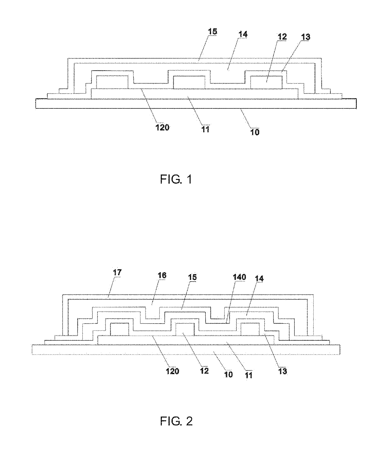
[0028]As shown in FIG. 1 it shows a encapsulation structure of an organic light emitting diode according to the present invention.
[0029]The encapsulation structure of the organic light emitting diode in this embodiment comprises: a substrate 10 and an organic light emitting diode element 11 formed on the substrate 10.
[0030]The organic light emitting diode element 11 generally comprises: a substrate, an anode, a Hole Injection Layer, a Hole Transporting Layer, an emitting material layer, an Electron Transport Layer, an Electron Injection Layer and a cathode. The principle of the organic light emitting diode element 11 is that the illumination generates due to the carrier injection and recombination under the electric field driving of the semiconductor material and the organic semiconductor illuminating material.
[0031]Specifically, the ITO electrode and the metal electrode are respectively employed as the anode and the cathode of the organic light emitting diode element 11. Under cert...
second embodiment
[0039]As shown in FIG. 2, it shows a encapsulation structure of an organic light emitting diode according to the present invention.
[0040]The difference between the encapsulation structure of the organic light emitting diode in the present embodiment and the aforesaid first embodiment is that the second organic thin film layer 14 is formed with a plurality of grooves 140 arranged at intervals by exposure and development processes thereon, so that the second inorganic thin film layer 14 is provided with the plurality of protrusions arranged at intervals. In practical, the second organic thin film layer 14 may be exposed and developed by a mask or a HTM mask to form the plurality of protrusions arranged at intervals.
[0041]The second inorganic thin film layer 15 is a continuous film structure and is prepared by depositing a thin film by chemical vapor deposition (CVD), which is coated on the first inorganic thin film layer 13, on the second organic thin film layer 14 and on the pluralit...
PUM
 Abstract
Description
Claims
Application Information
 - R&D
- Intellectual Property
- Life Sciences
- Materials
- Tech Scout
- Unparalleled Data Quality
- Higher Quality Content
- 60% Fewer Hallucinations
Browse by: Latest US Patents, China's latest patents, Technical Efficacy Thesaurus, Application Domain, Technology Topic, Popular Technical Reports.
© 2025 PatSnap. All rights reserved.Legal|Privacy policy|Modern Slavery Act Transparency Statement|Sitemap|About US| Contact US: help@patsnap.com