Antenna apparatus

a technology of antenna arrays and antennas, applied in the field of antenna apparatuses, can solve the problems of high insertion loss of existing phase shifters, high cost of manufacture of phased antenna arrays using phase shifters, etc., and achieve the effects of reducing parasitic and signal loss, reducing signal propagation paths, and reducing parasitic and signal losses

Active Publication Date: 2019-12-05
SOFANT TECH
View PDF0 Cites 10 Cited by
  • Summary
  • Abstract
  • Description
  • Claims
  • Application Information

AI Technical Summary

Benefits of technology

[0066]It may be that the antenna substrate is crystalline. It may be that the antenna substrate is monocrystalline. It may be that the antenna substrate is polycrystalline. By providing a crystalline (preferably monocrystalline) antenna substrate, signal losses can again be reduced, particularly at high signal frequencies.
[0067]It may be that the MEMS substrate and the (e.g. semiconductor) capping substrate (and in some embodiments, where provided, the antenna substrate) are arranged together in a stack (e.g. stacked one on top of the other). It may be that the (e.g. semiconductor) capping substrate is (e.g. vertically) offset from the MEMS substrate (e.g. in a stacking direction of the said capping substrate on the MEMS substrate). It may be that the antenna substrate is stacked on the sec

Problems solved by technology

In addition, existing phase shifters can have relatively high insertion losses.
Phased antenna arrays which use phase shifters can also be expensive to manufacture as t

Method used


Image

  • Antenna apparatus
  • Antenna apparatus
  • Antenna apparatus

Examples


Embodiment Construction

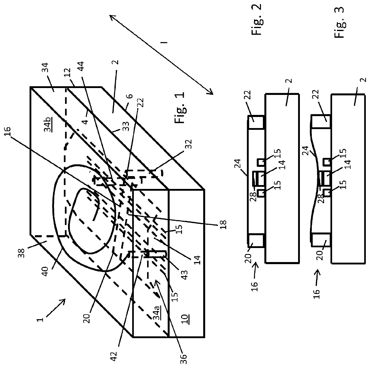
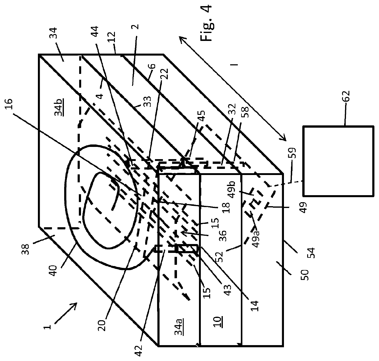
[0209]FIG. 1 shows an antenna module 1 of a phased antenna array, the antenna module having a (typically crystalline) semiconductor MEMS substrate (or wafer) 2 having a first surface 4 and a second surface 6 opposite the first surface 4, the first surface 4 supporting an electromagnetic (e.g. RF) signal conductor 14 together with a pair of ground conductors 15 which form a co-planar waveguide with the signal conductor 14 (although it is not necessary for a co-planar waveguide arrangement to provided; any suitable alternative arrangement may be provided, such as a microstrip arrangement in which a microstrip signal conductor 14 is provided on the first surface 4 of the substrate 2), and a plurality of reconfigurable MEMS switches, two of which 16, 18 are shown schematically in FIG. 1.

[0210]A first one of the MEMS switches 16 is shown more clearly in section in FIGS. 2 and 3. More specifically, the MEMS switch 16 is a capacitive switch comprising a conductive bridge 24 provided above ...


PUM

PropertyMeasurementUnit
Angleaaaaaaaaaa
Pressureaaaaaaaaaa
Poweraaaaaaaaaa

Abstract

The invention relates to antenna apparatus comprising: an antenna, a signal conductor and one or more RF MEMS switches, the antenna being conductively connected to the signal conductor, the MEMS switches and at least a portion of the signal conductor being supported by a crystalline MEMS substrate; and a capping substrate comprising a capping portion, wherein an enclosed volume is formed around the said MEMS switches between the capping portion and at least a portion of the crystalline MEMS substrate, and wherein the capping substrate comprises the said antenna.

Description

FIELD OF THE INVENTION[0001]The invention relates to antenna apparatus; methods of manufacturing antenna apparatus; a phased antenna array; a base station or a small, micro or femto cell infrastructure, a satellite communication device or a (typically wireless) backhaul, transmitter, receiver or transceiver comprising antenna apparatus; a base station comprising a phased antenna array; a mobile communications device comprising antenna apparatus; and a mobile communications device comprising a phased antenna array.BACKGROUND TO THE INVENTION[0002]Phased antenna arrays, in which the relative phases of electromagnetic signals received or to be transmitted by respective antennas of the array are controlled to effectively “steer” the antenna array in a desired direction and / or control their gain. One skilled in the art will appreciated that phased antenna arrays are electronically steered as distinct from mechanically steered (although phased antenna arrays may in addition be mechanicall...

Claims


Application Information

Patent Timeline
IPC IPC(8): H01Q1/22H01Q23/00H03H7/01B81C1/00B81B7/00H04B1/38H01Q3/30H01Q21/06
CPCH04B1/38H01Q23/00B81C1/00246H01Q21/065B81B7/0064B81C2203/0735H01Q3/30H01Q1/2283H03H7/0115B81C1/00269H01Q3/26H01Q3/2694H01Q3/28H01P1/18H01P1/22H01Q3/36
Inventor HARIDAS, NAKUL RAGHAVANANDWITHER, DAVID MICHAELSTEEL, VICTORZHOU, WEIIDDA, TONIOEL-RAYIS, ADMED OSMAN
Owner SOFANT TECH
Why Eureka
Try Eureka