
Germanium Silicon Tin Oxide Thin Films for Uncooled Infrared Detection

a technology of infrared detection and thin films, applied in the direction of optical radiation measurement, instruments, semiconductor devices, etc., can solve the problems of heat loss through radiation, heat loss through conduction/convection through the atmosphere surrounding the detector thermometer, and undesirable effects, and achieve low noise value, stable and high reproducibility properties, and high tcr value

Active Publication Date: 2019-12-26
RANA MUKTI +2
View PDF6 Cites 1 Cited by
  • Summary
  • Abstract
  • Description
  • Claims
  • Application Information

AI Technical Summary

Benefits of technology

This patent is about a new method to make thin films called Ge—Si—Sn—O that can increase the sensitivity of microbolometer devices. The technical effect of this invention is to improve the performance of microbolometer devices by using the new thin films.

Problems solved by technology

First, heat is lost through conduction / convection through the atmosphere surrounding the detector thermometer, that is described below.
Second, heat is lost through radiation.
However, the materials that are preferred for low heat loss also absorb less infrared radiation, which is not desirable.
This mechanism represents the ultimate limit on the performance of the detector.
Third, the heat is lost through thermal conduction through the supporting structure of the thermometer.
Since thermal noise power increases as the square root of heat conduction, the heat conduction to the environment poses the largest limit in terms of detection.
Also, lowering the heat capacity of the detector element by reducing the thickness of the detector structure leads to a large temperature change per radiation input, further reducing the effect of noise.
The main drawback found in all the materials is the low TCR which also ends up in lower responsivity and detectivity when they are used in microbolomter.

Method used


Image

  • Germanium Silicon Tin Oxide Thin Films for Uncooled Infrared Detection
  • Germanium Silicon Tin Oxide Thin Films for Uncooled Infrared Detection
  • Germanium Silicon Tin Oxide Thin Films for Uncooled Infrared Detection

Examples


Embodiment Construction

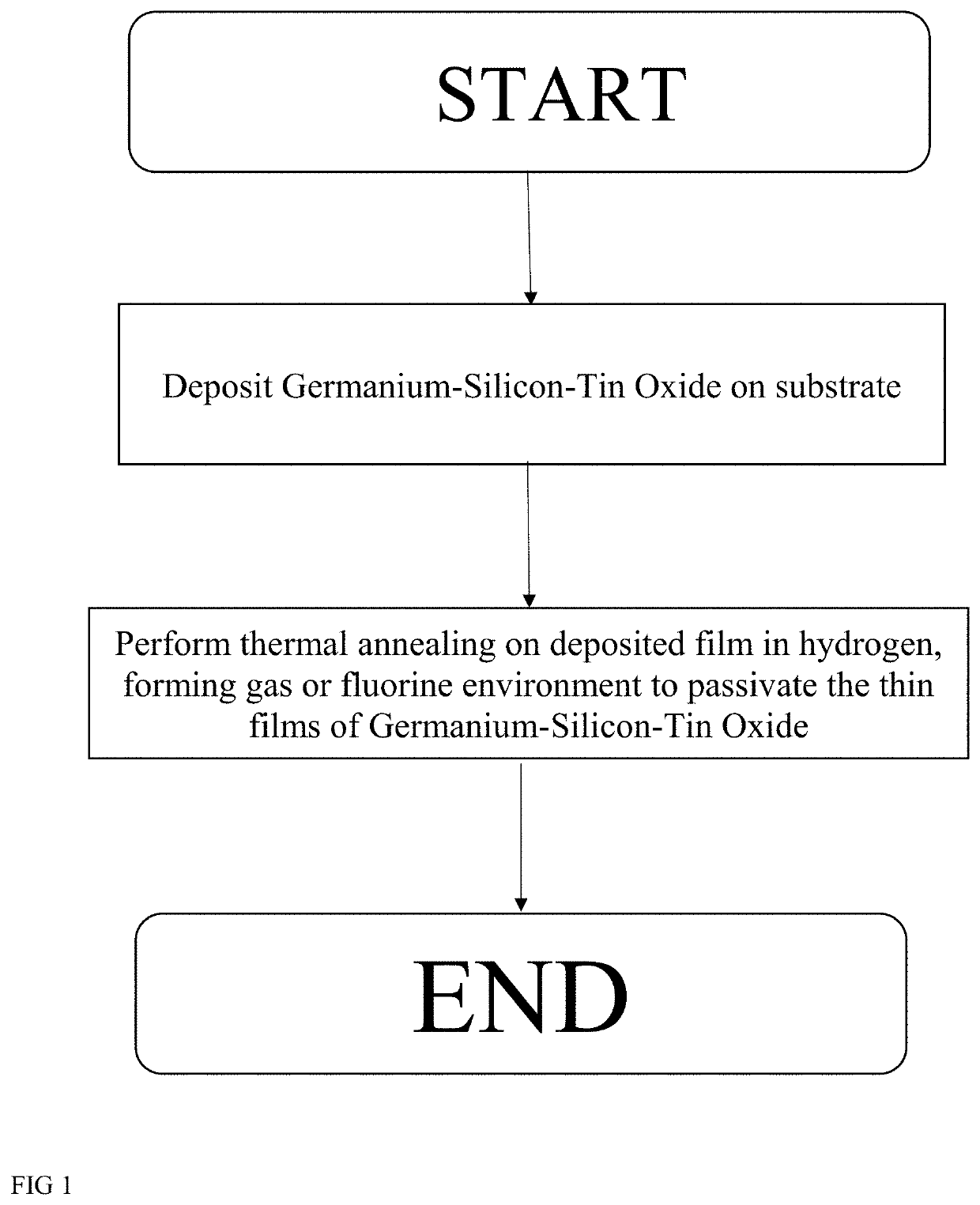
[0045]We present here the microbolometer elements and methods for forming the same. The sensing layer of microbolometer is fabricated using various atomic compositions of Germanium, Silicon, Tin and Oxygen to form an alloy of germanium-silicon-tin-oxide (Ge—Si—Sn—O). The variation in atomic composition in the alloy of Ge—Si—Sn—O will allow the materials' properties to be varied. The variation of the atomic composition in Ge—Si—Sn—O alloy will vary the fundamental material properties such as activation energy and carrier mobility. This way the key microbolometer device figures of merits such as resistivity, TCR, responsivity, absorption in IR region of interest, noise, detectivity, noise equivalent temperature difference are varied and optimized for better device performance.

[0046]Variation and optimization of atomic composition in the alloy of Ge—Si—Sn—O allow us to increase the room temperature TCR to a value which is significantly higher than the current reported values (from −2% / ...


PUM


Abstract

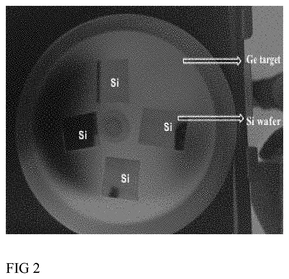
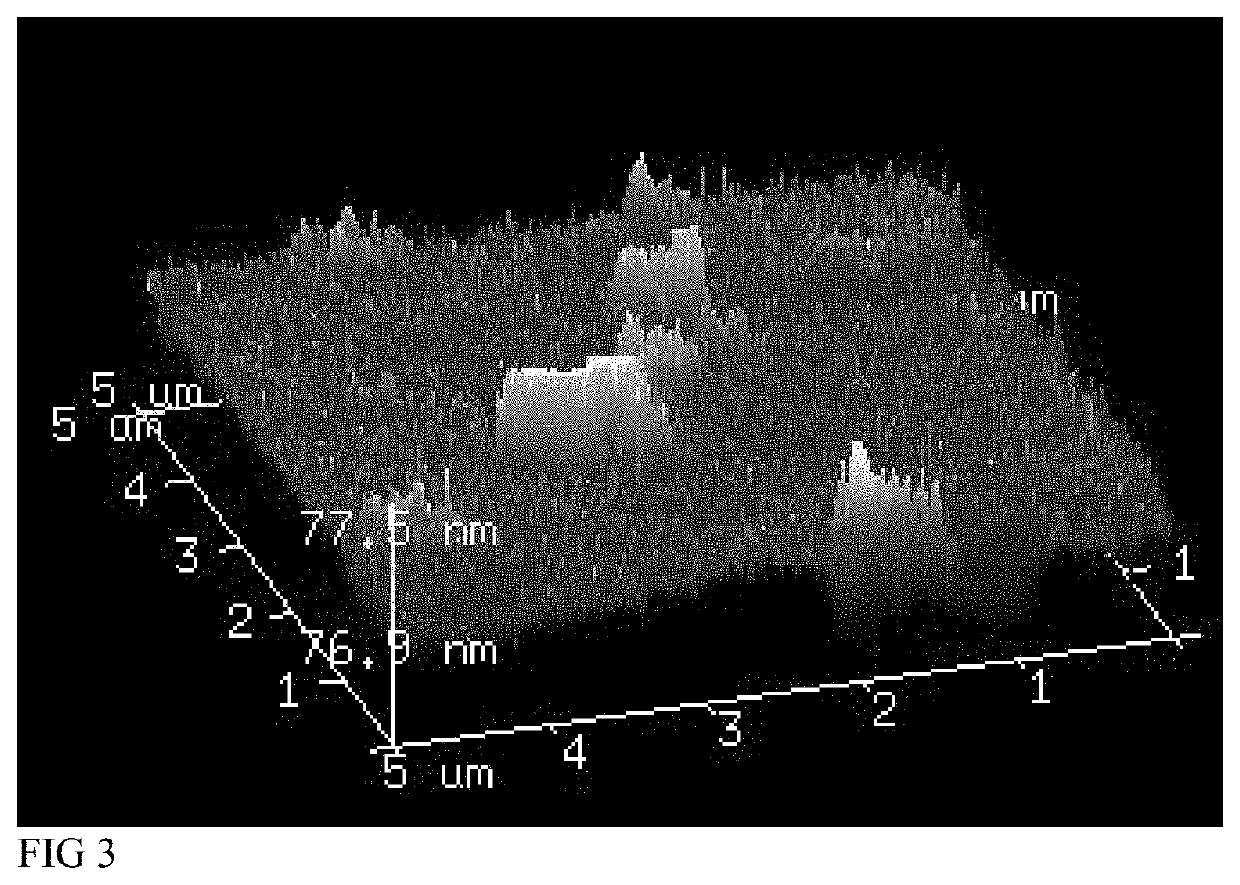
Microbolometer is a class of infrared detector whose resistance changes when the temperature changes. In this work, we deposited and characterized Germanium Silicon Oxide thin films mixed with Sn (Ge—Si—Sn—O) for uncooled infrared detection. Ge—Si—Sn—O were deposited by co-sputtering of Sn and Ge—Si targets in the Ar+O environment using a radio frequency sputtering system. Optical characterization shows that the absorption in Ge—Si—Sn—O was most sensitive in the wavelength ranges between 2.5-3.7 μm. The transmission data was further used to determine the optical energy band gap (0.22 eV) of the thin-film using Tauc's equation. We also found the variations of absorption coefficient (6592305.87 m−1-11615736.95 m−1), refractive index (2.5-4.0), and the extinction coefficient (2.31-5.73) for the wavelength ranges between 2.5-5.5 μm. The thin film's resistivity measured by the four point probe was found to be 142.55 Ω-cm and TCR was in the range of −4.9-−3.1 (% / k) in the temperature range 289-325 k.

Description

1. TECHNICAL FIELD OR FIELD OF INVENTION[0001]This invention relates to the Germanium Silicon Tin Oxide (Ge—Si—Sn—O) thin films for a microbolometer and a method of manufacturing thereof and an infrared detector or microbolometer using Ge—Si—Sn—O. It reports the deposition, characterization and properties of Ge—Si—Sn—O thin films for their electrical, optical, mechanical and morphological properties for microbolometer's sensing layer. Microbolometers are the infrared sensors which change their resistances when the temperature changes. The microbolometer operates in Midwave Infrared (MWIR, 3 to 5 μm) and Longwave Infrared (LWIR, 8 to 14 μm) wavelengths for detecting infrared (IR) radiation. The unique properties of Ge—Si—Sn—O will be used for uncooled IR detection.2. BACKGROUND OF THE INVENTION[0002]Thermal IR detectors are heated by the incident IR radiation and provide detection through the change in a measurable parameter. For these types of detectors, wavelengths of interest are ...

Claims


Application Information

Patent Timeline
IPC IPC(8): G01J5/24G01J5/08H01L31/024
CPCH01L31/024G01J5/0853G01J5/24G01J5/046G01J5/20
Inventor RANA, MUKTIMBABIT-TEBIT, LARINEDHAR, NIBIR
Owner RANA MUKTI
Learn More