Optical filter, optical filter system, spectrometer and method of fabrication thereof

a technology of optical filter and optical filter system, which is applied in the direction of optical radiation measurement, instruments, spectrometry/spectrophotometry/monochromators, etc., can solve the problem of reducing the bandwidth of the optical filter on which it is based, and achieves the effect of simple linear optical filter, easy manufacturing, and higher control of the aperture area

Active Publication Date: 2020-02-27
CSEM CENT SUISSE DELECTRONIQUE & DE MICROTECHNIQUE SA RECH & DEV
View PDF7 Cites 13 Cited by
  • Summary
  • Abstract
  • Description
  • Claims
  • Application Information

AI Technical Summary

Benefits of technology

[0027]In an embodiment of the invention said array of metallic nanostructures is a linear array of nanometer sized lamellas. The advantage of using lamellas for the metallic nanostructures is to provide a simple linear optical filter that is easy to manufacture. The transmission spectrum of the linear optical filter depends on the polarization of incident light. Measuring the polarization state of light may be useful for some applications.
[0028]In an embodiment of the invention said first substrate surface is a binary patterned surface. The binary structure enables a higher control of the area of the apertures during fabrication.
[0029]In an embodiment of the invention said first substrate surface is a sinusoidal patterned surface. The sinusoidal patterned surface has the advantage that it can originated with standard grating fabrication techniques such as laser interference lithography.
[0030]The invention concerns also an optical filter system comprising the optical transmission filter as described and comprises a detector array is fixed to said substrate Adapting a detector array such as a CMOS detector array allows proving a simple and compact optical filter systems that may be applied into a cheap spectrometer and / or provide a multispectral imager.
[0031]The invention relates also to a spectrometer comprising at least one optical transmission filter and / or at least one said optical transmission filter system said spectrometer having a spectral resolution lower than 30 nm, preferably lower than 20 nm, for incident light having a wavelength between 300 nm and 790 nm. A spectrometer based on the optical filter and filter system of the invention allows providing a compact, reliable and performant spectrometer at very low cost. The optical filter can be directly fabricated on a detector array without damaging its functionality.

Problems solved by technology

Without using a low index cladding it is not possible to reduce the bandwidth of an optical filter that is based on a nanostructured metallic layer.

Method used


Image

  • Optical filter, optical filter system, spectrometer and method of fabrication thereof
  • Optical filter, optical filter system, spectrometer and method of fabrication thereof
  • Optical filter, optical filter system, spectrometer and method of fabrication thereof

Examples


Embodiment Construction

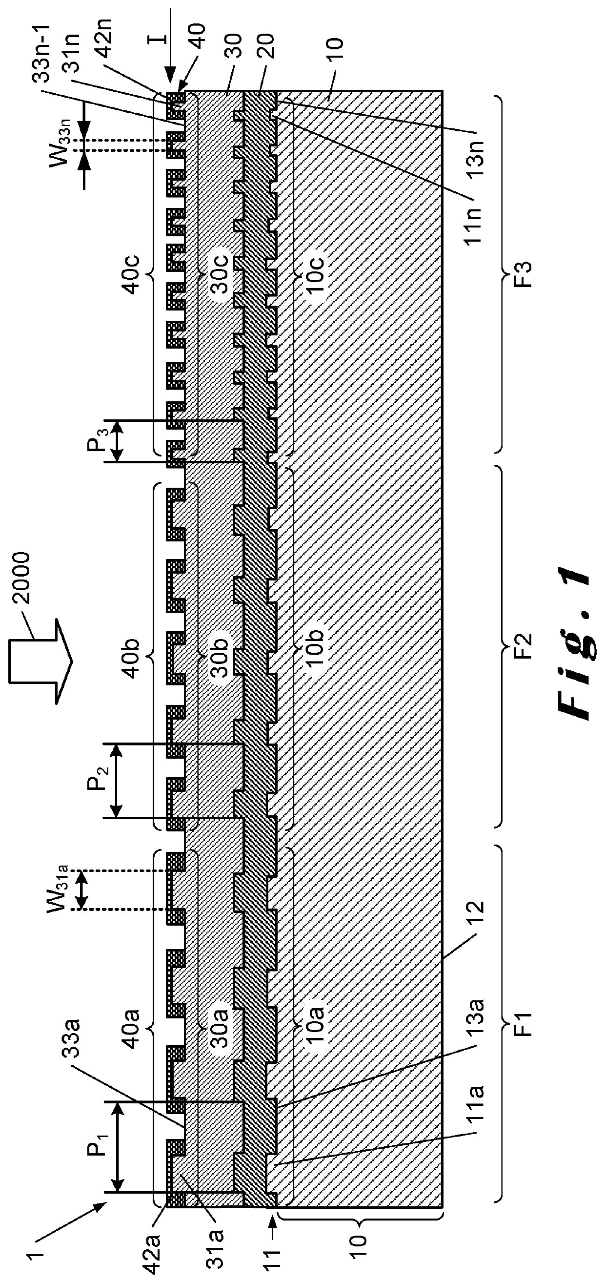
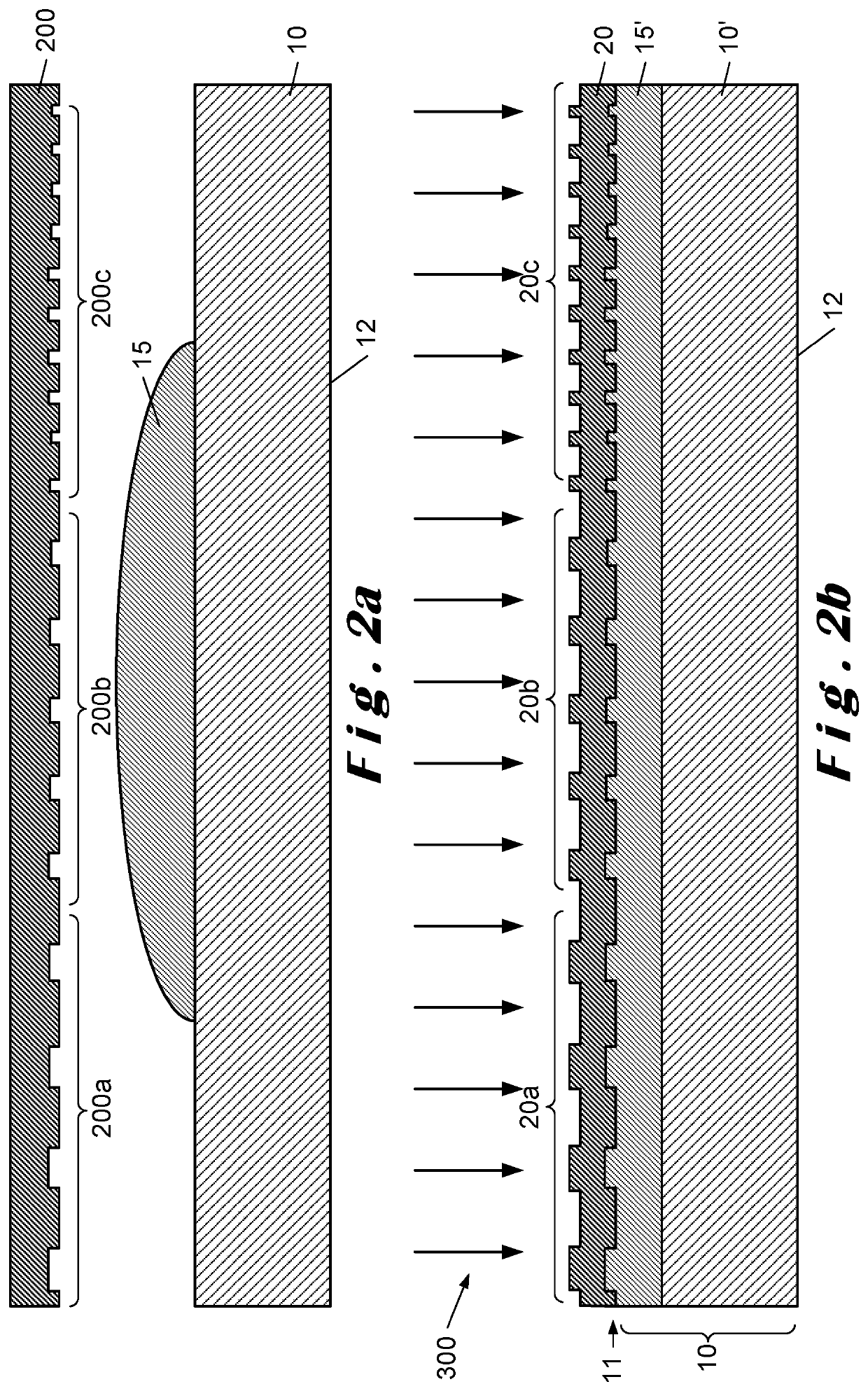
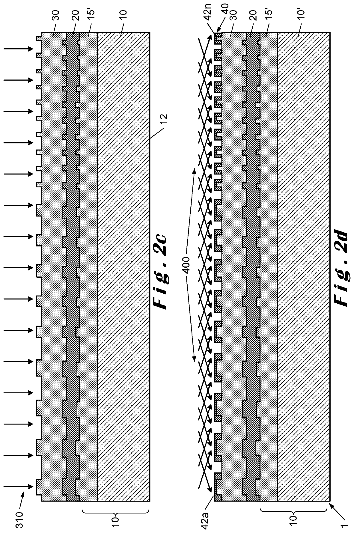
[0050]The present invention will be described with respect to particular embodiments and with reference to certain drawings but the invention is not limited thereto. The drawings described are only schematic and are non-limiting. In the drawings, the size of some of the elements may be exaggerated and not drawn on scale for illustrative purposes. The dimensions and the relative dimensions do not correspond to actual reductions to the practice of the invention.

[0051]It is to be noticed that the term “comprising” in the description and the claims should not be interpreted as being restricted to the means listed thereafter, i.e. it does not exclude other elements.

[0052]Reference throughout the specification to “an embodiment” means that a particular feature, structure or characteristic described in relation with the embodiment is included in at least one embodiment of the invention. Thus appearances of the wording “in an embodiment” or, “in a variant”, in various places throughout the ...


PUM

PropertyMeasurementUnit
refractive index n1aaaaaaaaaa
refractive index n2aaaaaaaaaa

Abstract

A nano-structured optical wavelength transmission filter is provided. The optical filter includes a patterned substrate on which a high refractive index dielectric waveguide is arranged. A low index dielectric layer is arranged on the high refractive index dielectric waveguide, on which an array of metallic nanostructures is arranged. The layers of the optical filter have conformal shapes defined by a patterned surface of the substrate. An optical filter system includes the optical transmission filter and a detector array fixed to the substrate. A spectrometer includes at least one optical transmission filter and/or at least one said optical transmission filter system, and has a spectral resolution of lower than 30 nm for incident light having a wavelength between 300 nm and 790 nm. A method of fabrication of an optical filter, an optical filter system and a spectrometer is also described.

Description

TECHNICAL FIELD[0001]The invention relates to the field of transmission optical filters, optical detectors and spectrometers comprising such filters and optical detectors.[0002]More precisely the invention relates to highly transmitting optical filters and such filter arrays having a band-pass with low bandwidth, and comprising a nanostructured substrate and waveguides arranged on such structured substrates. The invention relates also to a miniature spectrometer configured for the market of consumer electronics. The invention encompasses also a method of fabrication of an optical transmission filter having a low bandwidth.[0003]The invention also relates to a method of fabrication of the transmission optical filter and optical detector.BACKGROUND OF THE ART[0004]The use of optical filters, in particular transmission filters, is important in optical components and optical instruments and systems. For example optical filters combined are often combined with optical detectors, in visio...

Claims


Application Information

Patent Timeline
Patent Type & Authority Applications(United States)
IPC IPC(8): G01J3/51G01J3/28G02B5/20
CPCG01J3/51G02B5/201G02B5/208G01J3/28G01J3/02G01J3/0205G01J3/36G02B5/204B82Y20/00G02B5/008H01L31/02162H01L27/14621G02B5/1866G01J3/0256G01J3/0259G01J3/0229G01J2003/1213G01J2003/1217G01J3/2803G01J2003/2806G01J2003/1861G01J3/1895G02B5/20
Inventor GALLINET, BENJAMINQUARANTA, GIORGIOBASSET, GUILLAUME
Owner CSEM CENT SUISSE DELECTRONIQUE & DE MICROTECHNIQUE SA RECH & DEV
Why Eureka
Try Eureka