
Bifacial p-type perc solar cell and module, system, and preparation method thereof

a solar cell and p-type technology, applied in the field of solar cells, can solve the problems of complex process of manufacturing a bifacial n-type cell, high price of n-type silicon wafer, and limited photoelectric conversion efficiency, so as to simplify the laser process and printing process, and facilitate industrial production. scale-up, the effect of reducing the difficulty of debugging the printing devi

Active Publication Date: 2020-04-16
GUANGDONG AIKO SOLAR ENERGY TECH CO LTD +1
View PDF0 Cites 0 Cited by
  • Summary
  • Abstract
  • Description
  • Claims
  • Application Information

AI Technical Summary

Benefits of technology

The present invention provides a bifacial P-type PERC solar cell that has a simple structure, low cost, easy popularization, and high photoelectric conversion efficiency. Additionally, the invention provides a method for preparing the solar cell and a solar cell module with the same features.

Problems solved by technology

However, as passivation is not provided at the rear surface of the silicon wafer, the increase in photoelectric conversion efficiency is still limited.
However, the price of an N-type silicon wafer is high, and the process of manufacturing a bifacial N-type cell is complicated.

Method used


Image

  • Bifacial p-type perc solar cell and module, system, and preparation method thereof
  • Bifacial p-type perc solar cell and module, system, and preparation method thereof
  • Bifacial p-type perc solar cell and module, system, and preparation method thereof

Examples


embodiment 1

[0122](1) forming textured surfaces at a front surface and a rear surface of a silicon wafer, the silicon wafer being P-type silicon;

[0123](2) performing diffusion on the silicon wafer to form an N-type emitter;

[0124](3) removing phosphosilicate glass on the front surface and peripheral p-n junctions formed during the diffusion;

[0125](4) depositing an aluminum oxide (Al2O3) film on the rear surface of the silicon wafer;

[0126](5) depositing a silicon nitride film on the rear surface of the silicon wafer;

[0127](6) depositing a silicon nitride film on the front surface of the silicon wafer;

[0128](7) performing laser grooving in the rear surface of the silicon wafer to form the first laser grooving region, wherein the first laser grooving region includes a plurality of sets of first laser grooving units that are horizontally arranged, each of the sets of the first laser grooving units includes one or more first laser grooving bodies arranged horizontally, and the laser grooving bodies e...

embodiment 2

[0135](1) forming textured surfaces at a front surface and a rear surface of a silicon wafer, the silicon wafer being P-type silicon;

[0136](2) performing diffusion on the silicon wafer to form an N-type emitter;

[0137](3) removing phosphosilicate glass on the front surface and peripheral p-n junctions formed during the diffusion and polishing the rear surface of the silicon wafer;

[0138](4) depositing an aluminum oxide (Al2O3) film on the rear surface of the silicon wafer;

[0139](5) depositing a silicon nitride film on the rear surface of the silicon wafer;

[0140](6) depositing a silicon nitride film on the front surface of the silicon wafer;

[0141](7) performing laser grooving in the rear surface of the silicon wafer to form a first laser grooving region, a second laser grooving region and a third laser grooving region, wherein the first laser grooving region includes a plurality of sets of horizontally-arranged first laser grooving units, each of the sets of first laser grooving units ...

embodiment 3

[0150](1) forming textured surfaces at a front surface and a rear surface of a silicon wafer, the silicon wafer being P-type silicon;

[0151](2) performing diffusion on the silicon wafer to form an N-type emitter;

[0152](3) removing phosphosilicate glass on the front surface and peripheral p-n junctions formed during the diffusion;

[0153](4) depositing an aluminum oxide (Al2O3) film on the rear surface of the silicon wafer;

[0154](5) depositing a silicon nitride film on the rear surface of the silicon wafer;

[0155](6) depositing a silicon nitride film on the front surface of the silicon wafer;

[0156](7) performing laser grooving in the rear surface of the silicon wafer to form a first laser grooving region, wherein the first laser grooving region includes a plurality of sets of horizontally-arranged first laser grooving units, each of the sets of first laser grooving units includes one or more horizontally-arranged first laser grooving bodies, and the first laser grooving bodies each have ...


PUM

PropertyMeasurementUnit
widthaaaaaaaaaa
lengthaaaaaaaaaa
lengthaaaaaaaaaa

Abstract

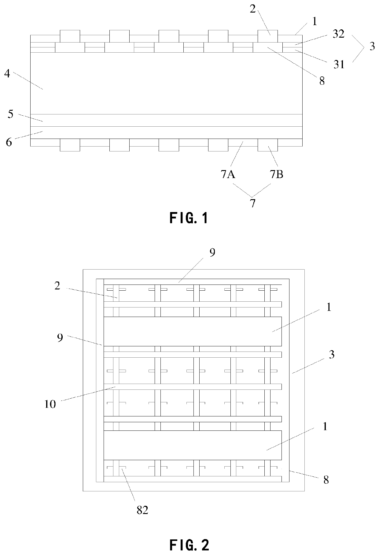
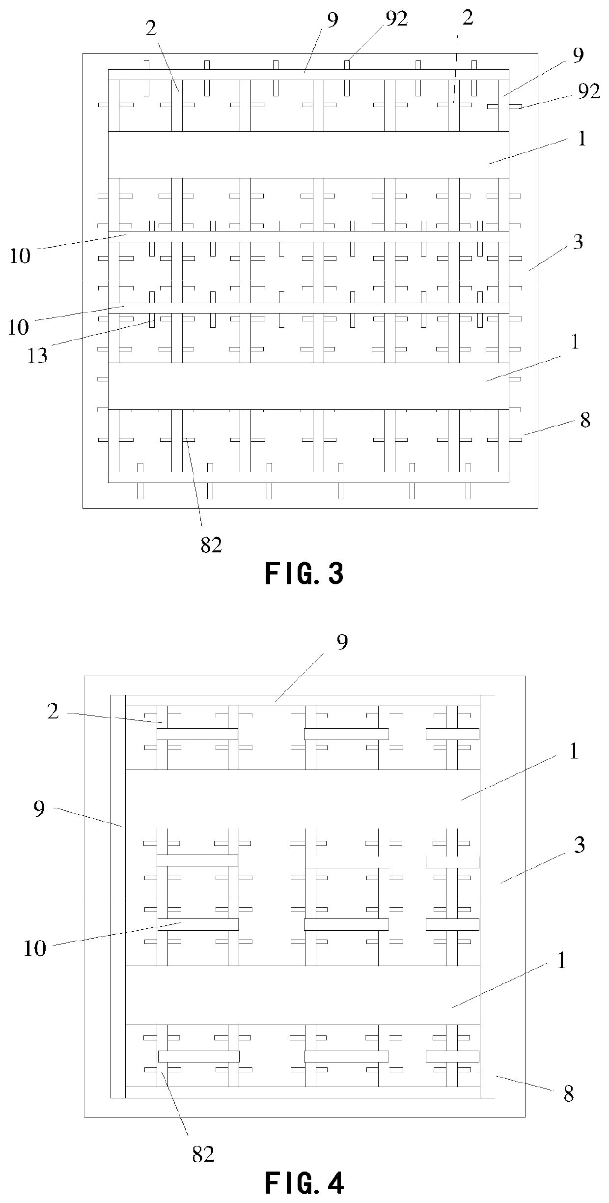
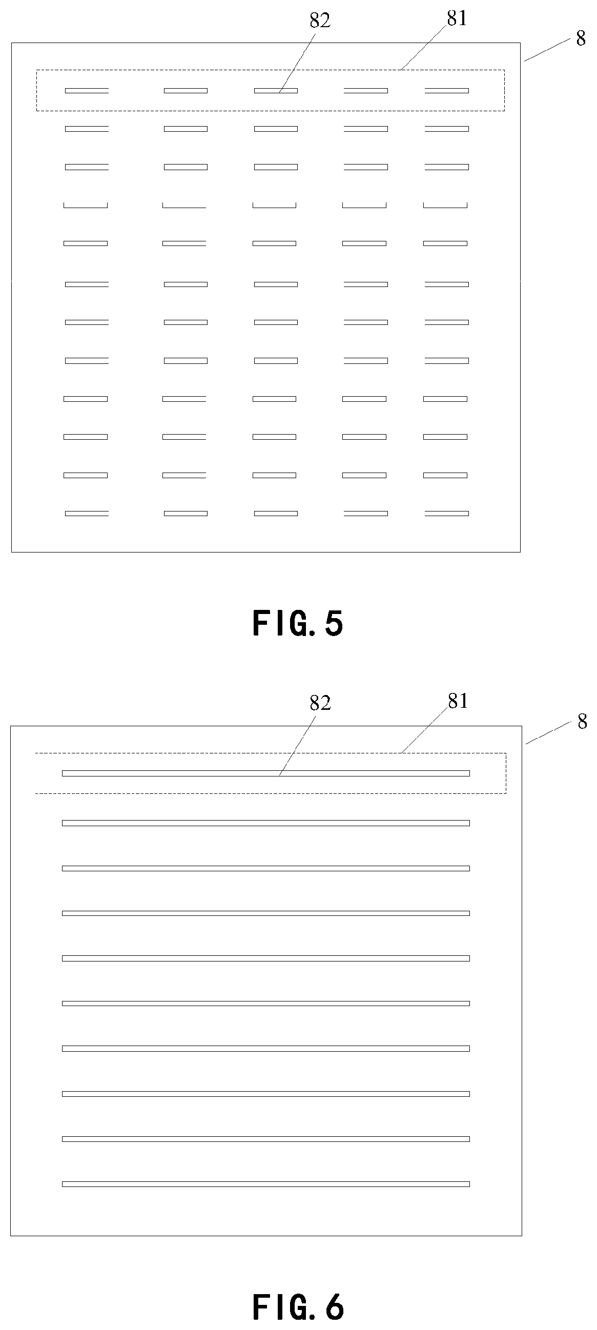
Provided are a bifacial P-type PERC solar cell, preparation method, module and system. The bifacial P-type PERC solar cell consecutively comprises a rear silver electrode (1), rear aluminum grid lines (2), a rear passivation layer (3), P-type silicon (4), an N-type emitter (5), a front silicon nitride film (6), and a front silver electrode (7); the rear silver electrode (1) is perpendicularly connected with the rear aluminum grid lines (2), grid line backbones (10) are disposed on the rear aluminum grid lines (2), an outer aluminum grid frame (9) is disposed around the rear aluminum grid lines (2), the grid line backbones (10) are connected with the rear aluminum grid lines (2), and the outer aluminum grid frame (9) is connected with the rear aluminum grid lines (2) and the rear silver electrode (1); a first laser grooving region (8) is formed in the rear passivation layer (3) with laser grooving, and the rear aluminum grid lines (2) are connected to the P-type silicon (4) via the first laser grooving region (8); the first laser grooving region (8) includes a plurality of sets of first laser grooving units (81) arranged horizontally, each of the sets of first laser grooving units (81) includes one or more first laser grooving bodies (82) arranged horizontally, and the rear aluminum grid lines (2) are perpendicular to the first laser grooving bodies (82). The solar cell is simple in structure, low in cost and easy to popularize, and has a high photoelectric conversion efficiency.

Description

FIELD OF THE DISCLOSURE[0001]The present invention relates to the field of solar cells, and in particular to a bifacial P-type PERC solar cell, a method of preparing the bifacial P-type PERC solar cell, a solar cell module that employs the bifacial P-type PERC solar cell, and a solar system that employs the bifacial P-type PERC solar cell.BACKGROUND OF THE DISCLOSURE[0002]A crystalline silicon solar cell is a device that effectively absorbs solar radiation energy and converts light energy into electrical energy through the photovoltaic effect. When sunlight reaches the p-n junction of a semiconductor, new electron-hole pairs are generated. Under the action of the electric field of the p-n junction, the holes flow from the N zone to the P zone, and the electrons flow from the P zone to the N zone, generating current upon switching on a circuit.[0003]In a conventional crystalline silicon solar cell, surface passivation is basically only performed at the front surface, which involves d...

Claims


Application Information

Patent Timeline
Patent Type & Authority Applications(United States)
IPC IPC(8): H01L31/0224H01L31/068H01L31/18H01L31/0236
CPCH01L31/0684H01L31/02366H01L31/1804H01L31/1868H01L31/022433H01L31/022425H01L31/022441Y02E10/547Y02P70/50H01L31/068H01L31/1864H01L21/76H01L31/047Y02E10/50
Inventor LIN, KANG-CHENGFANG, JIEBINCHEN, GANG
Owner GUANGDONG AIKO SOLAR ENERGY TECH CO LTD
Learn More