Semiconductor photodetector assembly

a technology of photodetectors and semiconductors, applied in the direction of semiconductor devices, electrical equipment, basic electric elements, etc., can solve the problems of reducing the capacitance of junctions and reducing the response time, and achieve the effect of reducing the cost factor of conventional ingaas photodetectors and high performan

Active Publication Date: 2020-07-09
ANALOG DEVICES INC
View PDF0 Cites 8 Cited by
  • Summary
  • Abstract
  • Description
  • Claims
  • Application Information

AI Technical Summary

Benefits of technology

[0006]The photodetector assembly can operate as a photodiode, a phototransistor, or can include both a photodiode and a phototransistor. The photodetector described ...

Problems solved by technology

This can reduce the response time because the additional reverse bias can incr...

Method used


Image

  • Semiconductor photodetector assembly
  • Semiconductor photodetector assembly
  • Semiconductor photodetector assembly

Examples


Embodiment Construction

[0021]Photodetectors can be combined into image sensing devices, such as focal plane arrays (FPAs), and used in numerous automobile, space, and military applications. For example, one application includes remote sensing using light pulses emitted for example by lasers and reflected by distant objects can be referred to as LIAR (light detection and ranging). A LIDAR receiver can include an optical receiver having a photodiode (PD) as a receiving element, and a transimpedance amplifier (TIA), for example a shunt-feedback amplifier, which converts the photocurrent from the receiving photodiode into a voltage.

[0022]LIDAR systems can use short-wave infrared light (SWIR), such as wavelengths greater than about 1 micrometer (μm) to about 3 μm. In these applications, conventional photodetectors use indium gallium arsenide (InGaAs), photodiode (PDs) for achieving high performance at a wavelength of about 1.5 μm. However, the high cost of InGaAs PDs have delayed their adoption in different co...


PUM


Abstract

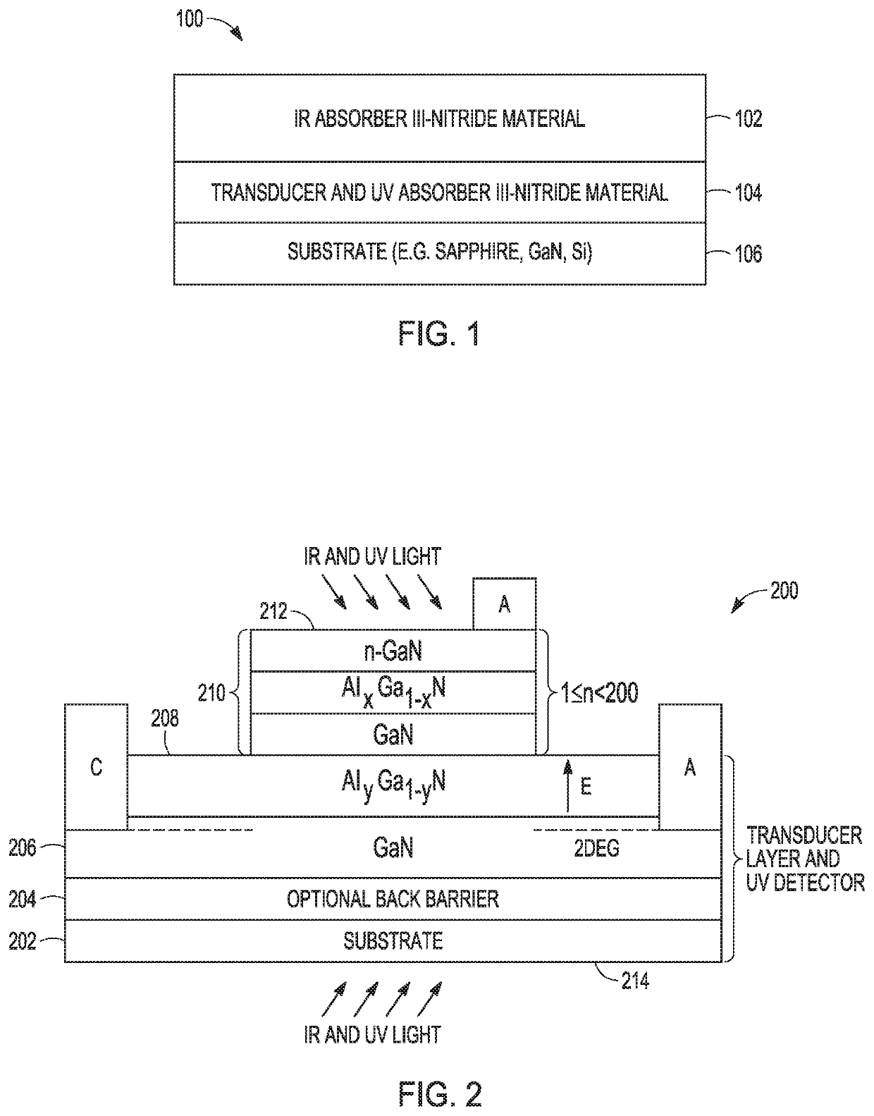
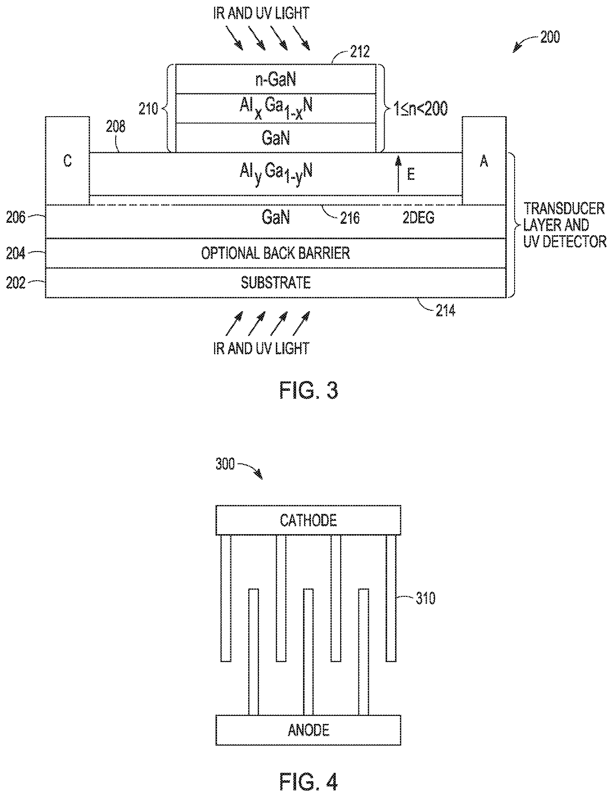
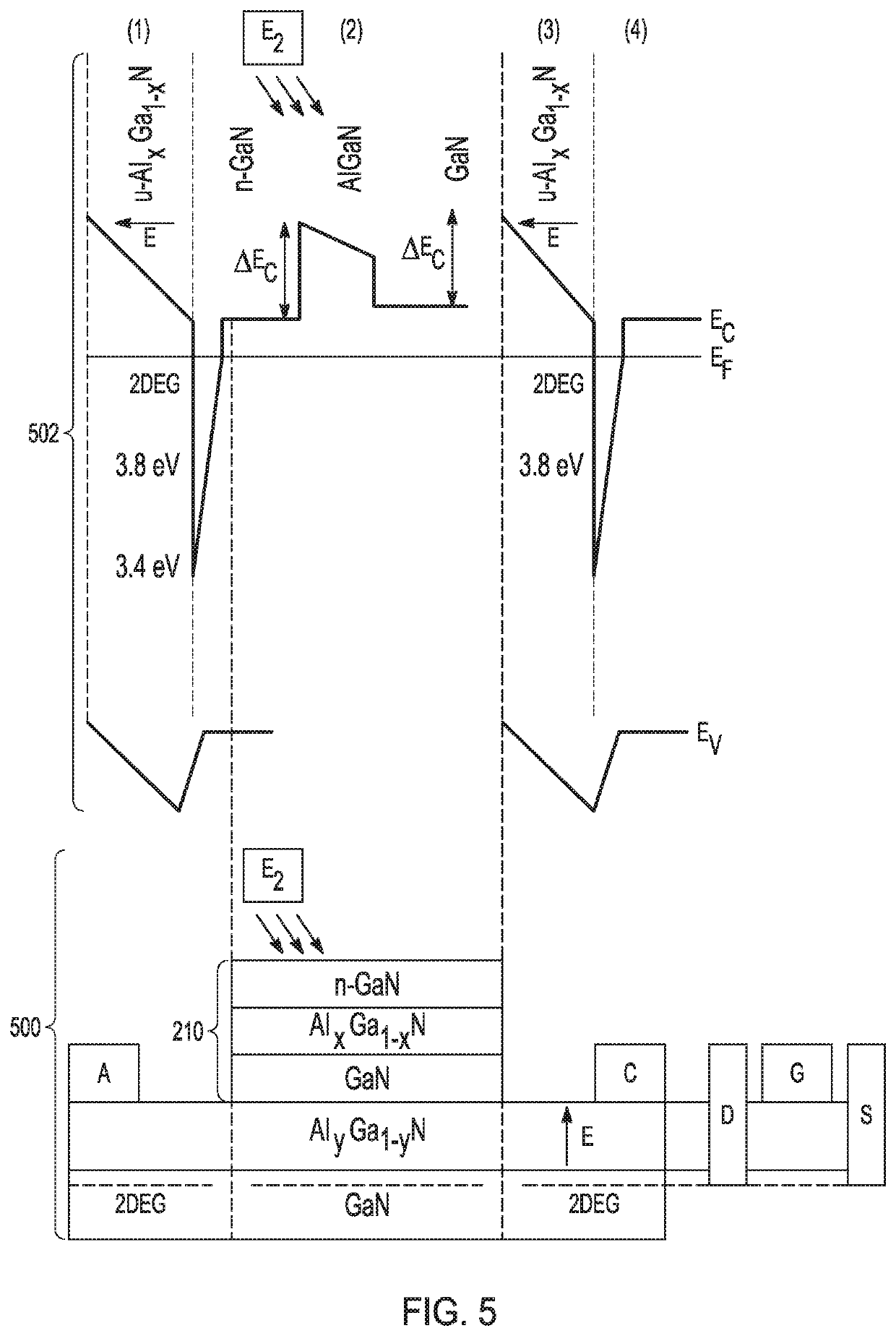
Techniques to use energy band gap engineering (or band offset engineering) to produce a photodetector semiconductor assembly that can be tuned to absorb light in one or more wavelengths. For example, the assembly can be tuned to receive infrared (IR) and/or ultraviolet (UV) light. The photodetector assembly can operate as a photodiode, a phototransistor, or can include both a photodiode and a phototransistor.

Description

CLAIM OF PRIORITY[0001]This application claims the benefit of priority of U.S. Provisional Patent Application Ser. No. 62 / 789,829, titled “SEMICONDUCTOR PHOTODETECTOR ASSEMBLY” to Mohamed Azize, filed on Jan. 8, 2019, the entire contents of which being incorporated herein by reference.FIELD OF THE DISCLOSURE[0002]This document pertains generally, but not by way of limitation, to photodetector assemblies and methods.BACKGROUND[0003]A photodiode is typically a PN junction or PIN structure. When a photon of sufficient energy strikes the diode, it can create an electron-hole pair. This mechanism is also known as the inner photoelectric effect. If the absorption occurs in the junction's depletion region, or one diffusion length away from it, these carriers are swept from the junction by the built-in electric field of the depletion region. Thus, holes move toward the anode, and electrons move toward the cathode, and a photocurrent is produced.[0004]When used in zero bias or photovoltaic m...

Claims


Application Information

Patent Timeline
IPC IPC(8): H01L31/0304H01L31/0352H01L31/0224H01L31/109H01L31/112H01L31/18H01L31/0232
CPCH01L31/02327H01L31/03048H01L31/1848H01L31/022408H01L31/035272H01L31/109H01L31/1123H01L31/035245H01L31/035281H01L31/1129H01L31/1013
Inventor AZIZE, MOHAMED
Owner ANALOG DEVICES INC
Why Eureka
Try Eureka