Initiating and monitoring the evolution of single electrons within atom-defined structures

a single electron and atom technology, applied in the field ofatomic structures, can solve the problems of affecting the investigation of systems, slow and computationally expensive, and impede the use of samples generated,

Active Publication Date: 2020-08-06
QUANTUM SILICON INC
View PDF0 Cites 1 Cited by
  • Summary
  • Abstract
  • Description
  • Claims
  • Application Information

AI Technical Summary

Benefits of technology

[0012]A method for the patterning and control of single electrons on a surface is provided that includes implementing scanning tunneling microscopy hydrogen lithography with a scanning probe microscope to form charge structures with one or more confined charges; performing a series of field-free atomic force microscopy measurements on the charge structures with different tip heights, where interaction between the tip and th...

Problems solved by technology

This step is typically implemented using Markov Chain Monte Carlo (MCMC) software methods that are slow and computationally-expensive and do not guarantee the in...

Method used


Image

  • Initiating and monitoring the evolution of single electrons within atom-defined structures
  • Initiating and monitoring the evolution of single electrons within atom-defined structures
  • Initiating and monitoring the evolution of single electrons within atom-defined structures

Examples


example 1

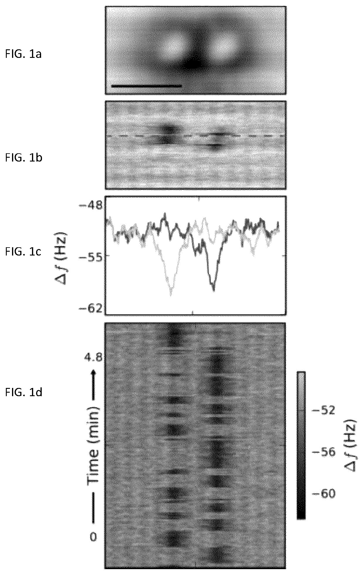
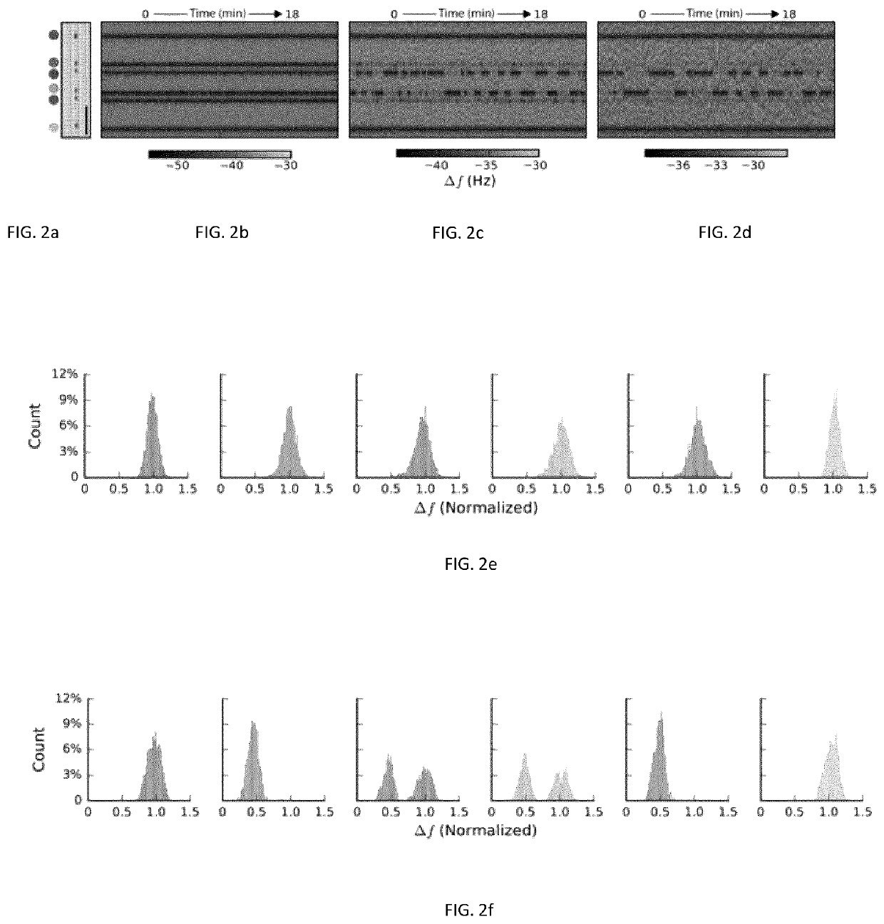
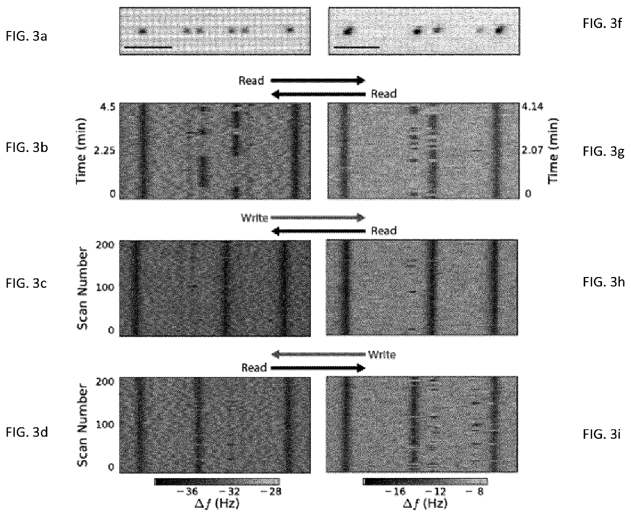
[0043]Experimental Setup—Experiments were performed using an Omicron LT STM / AFM head operating at 4.5 K and ultrahigh vacuum (−10 Torr). Tips were created from polycrystalline tungsten wire that was chemically etched, then sharpened, cut, and welded to a qPlus sensor using a focused ion beam. This fabrication technique reduces the sensors' mass loading to improve its quality factor. An additional electrode on the sensor was used to supply tunneling current. Tips were further processed with electron bombardment to remove the surface oxide, and sharpened by nitrogen etching while performing field ion microscopy. In-situ tip processing was performed by making controlled contacts with the tip to the sample surface, where previous reports have indicated likely results in a silicon apex. Samples were cleaved from (100)-oriented Si crystals that are highly As-doped (1.5×10⁹ atom cm−3). After degassing at 600° C. for 12 hours, samples were flash annealed to temperatures as high as 1250° C. ...


PUM


Abstract

A method for the patterning and control of single electrons on a surface is provided that includes implementing scanning tunneling microscopy hydrogen lithography with a scanning probe microscope to form charge structures with one or more confined charges; performing a series of field-free atomic force microscopy measurements on the charge structures with different tip heights, where interaction between the tip and the confined charge are elucidated; and adjusting tip heights to controllably position charges within the structures to write a given charge state. The present disclose also provides a Gibb's distribution machine formed with the method for the patterning and control of single electrons on a surface. A multi bit true random number generator and neural network learning hardware formed with the above described method are also provided.

Description

RELATED APPLICATIONS[0001]This application claims priority benefit of U.S. Provisional Application Ser. No. 62 / 564,734; filed 28 Sep. 2017; the contents of which are hereby incorporated by reference.FIELD OF THE INVENTION[0002]The present invention in general relates to atomic structures, and in particular to the manipulation of individual electrons, the spontaneous rearrangements of electrons and the readout of electronic configurations in defined atomic structures.BACKGROUND OF THE INVENTION[0003]Neural Networks formed of interconnected information processing nodes are powerful machine-learning tools. Neural Networks turn vast amounts of unorganized data into useful information, and are increasingly used for a variety of important applications illustratively including: character recognition, speech recognition, automation translation, facial recognition or stock market prediction, to cite just a few examples.[0004]Before a neural network can be put to work, the neural network must...

Claims


Application Information

Patent Timeline
IPC IPC(8): G01Q80/00G01Q60/10G01Q60/24G01Q30/10G01Q70/14G06N3/08G06N3/04
CPCG01Q80/00G01Q60/24G01Q60/10G06N3/08G01Q70/14G01Q30/10G06N3/04G06N20/10H01L29/7613H01L29/66977H01L29/66984B82Y10/00G06N3/065G06N3/047G06N7/01G06N3/044
Inventor WOLKOW, ROBERTRASHIDI, MOHAMMADVINE, WYATTDIENEL, THOMASLIVADARU, LUCIANHUFF, TALEANARETALLICK, JACOBWALUS, KONRAD
Owner QUANTUM SILICON INC
Why Eureka
Try Eureka