A Hybrid Flat Panel Detector For Cone Beam CT Systems

a technology of cone beam and detector, applied in the field of xray detectors, can solve the problems of image quality degradation and image quality degradation, and achieve the effects of improving primary transmission, efficient scatter rejection capability, and improving the performance of flat panel x-ray detectors

Active Publication Date: 2020-08-27
UNIV OF COLORADO THE REGENTS OF
View PDF0 Cites 7 Cited by
  • Summary
  • Abstract
  • Description
  • Claims
  • Application Information

AI Technical Summary

Benefits of technology

[0010]The present invention relates generally to X-ray detectors and more particularly to a system and a method for using anti-scattering grids to significantly enhance the performance of flat panel X-ray detector. In one embodiment, the invention relates to a novel flat panel detector, which integrates a two dimensional (2D) antiscatter grid and a phosphor layer with the detector's pixel array. In one embodiment, said two dimensional anti scatter grid of apertures separated by radio-opaque septa, placed in contact with the flat panel detector (FPD). In one embodiment, Direct Metal Laser Sintering (DMLS) is used construct a 2D aperture array, such that each aperture may be precisely aligned towards the x-ray focal spot. In one embodiment, said aperture array has septal thickness down to 100 microns. In one embodiment, lithographic techniques are used construct a 2D aperture array, such that each aperture may be precisely aligned towards the x-ray focal spot. In one embodiment, said 2D aperture array has a septal thickness down to 100 microns. In one embodiment, the presence of thin septa combined with the absence of inter-septal spacers improves primary transmission, while the two dimensional aperture array provides efficient scatter rejection capability at levels not achievable with current scatter rejection devices.
[0011]In one embodiment, the invention relates to a signal adjustment mechanism to counteract the shadow effect that the antiscatter grid may have on the detector. In one embodiment, the flat panel detector is be redesigned such that the 2D grid is directly placed on the phosphor layer. In one embodiment, the normal flat panel detector continuous phosphor layer is replaced with a pixelated phosphor layer. In one embodiment, said pixels in the phosphor are separated with reflective septa, preventing diffusion of visible light photons neighboring detector pixels. In one embodiment, said 2D grid comprises at least one wall which is aligned with the septa in the phosphor layer, minimizing the “inactive” area of the flat panel detector. It is believed that benefit cannot be achieved with the conventional approach where the grid is mounted on the top of the protective detector cover because the walls cannot be perfectly aligned with the septa of phosphor layer. It is believed that advantages of this hybrid design over existing flat panel detectors include: Pixelated phosphor structure reduces cross-talk between detector pixels, improves spatial resolution; 2D grid provides better scatter absorption and improved primary x-ray transmission with respect to conventional antiscatter grids. In return, it reduces noise in x-ray images. Integration of pixelated phosphor with the 2D antiscatter grid reduces the percentage of “inactive” detector area, thus more primary x-rays will be detected by the detector.
[0019]As used herein, the term “sintered element” is used herein to describe a material which may be used as a source material in a 3D printing process, such as direct metal laser sintering. Selective laser sintering allows for a large design freedom. Having a structural element that is built by selective laser sintering, the grid may be a highly complex three-dimensional structure that is not easily achievable by conventional moulding or milling techniques. Therein, the technology of selective laser sintering, sometimes also known as direct metal laser sintering, is not any longer a prototype technology but becomes a production technology for the manufacturing of three-dimensional devices with demanding geometries.
[0021]As used herein, the term “metal oxide semiconductor (CMOS)” is used herein to describe a technology for constructing integrated circuits. CMOS is also sometimes referred to as complementary-symmetry metal-oxide-semiconductor (or COS-MOS). The words “complementary-symmetry” refer to the fact that the typical design style with CMOS uses complementary and symmetrical pairs of p-type and n-type metal oxide semiconductor field effect transistors (MOSFETS) for logic functions. Two important characteristics of CMOS devices are high noise immunity and low static power consumption.

Problems solved by technology

As a result, the image quality can be deteriorated.
Although, 2D grid's height (or grid ratio) can be increased to reduce the transmission of scatter, such a grid design will lead to other technical and practical challenges, which deteriorates image quality.

Method used


Image

  • A Hybrid Flat Panel Detector For Cone Beam CT Systems
  • A Hybrid Flat Panel Detector For Cone Beam CT Systems
  • A Hybrid Flat Panel Detector For Cone Beam CT Systems

Examples


example 1

[0209]In one embodiment, the invention relates to a two-dimensional antiscatter grid, wherein said two-dimensional antiscatter grid is installed on top of a flat panel detector protective cover. In one embodiment, said two-dimensional antiscatter grid is described in FIG. 20, FIG. 21, and FIG. 22. In one embodiment, some basic x-ray transmission characteristics of the two-dimensional antiscatter grid are described in Example 2. In one embodiment, said hybrid flat panel detector is described in Example 3 & Example 4. In one embodiment, said two-dimensional antiscatter grid unique qualities and grid parameters are described in Example 5 & Example 6. In one embodiment, a method to correct scatter using a 2D antiscatter grid is described in Example 7. In one embodiment, an illustration of a pixelated scintillator is found in FIG. 20, FIG. 21, and FIG. 22. A more expansive description of one embodiment of the current invention is described in Example 2. Previous explorations of antiscatt...

example 2

Transmission Characteristics of a Two Dimensional Antiscatter Grid Prototype for CBCT [102]

[0227]Aim:

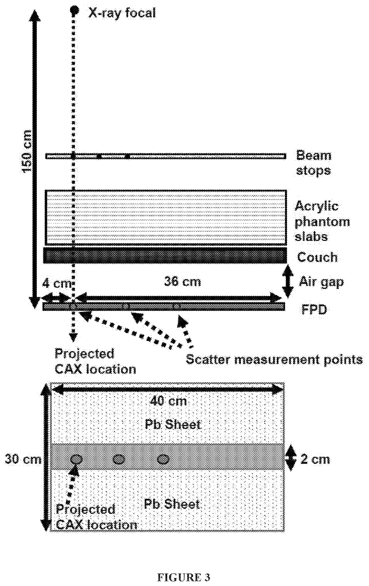
[0228]High fraction of scattered radiation in CBCT imaging degrades CT number accuracy and visualization of low contrast objects. To suppress scatter in CBCT projections, a focused, two-dimensional antiscatter grid (2D ASG) prototype was developed. In this Example, the primary and scatter transmission characteristics of the 2D ASG prototype aimed for linac mounted, offset detector geometry CBCT systems in radiation therapy, are described and compared its performance to a conventional one-dimensional ASG (1D ASG).

[0229]Methods:

[0230]The 2D ASG is an array through-holes separated by 0.1 mm septa that was fabricated from tungsten using additive manufacturing techniques. Through-holes' focusing geometry was designed for offset detector CBCT in Varian TrueBeam system. Two types of ASGs were evaluated: a) a conventional 1D ASG with a grid ratio of 10, b) the 2D ASG prototype with a grid ra...

example 3

Configuration of Current X-Ray Flat Panel Detectors and 1D ASGS

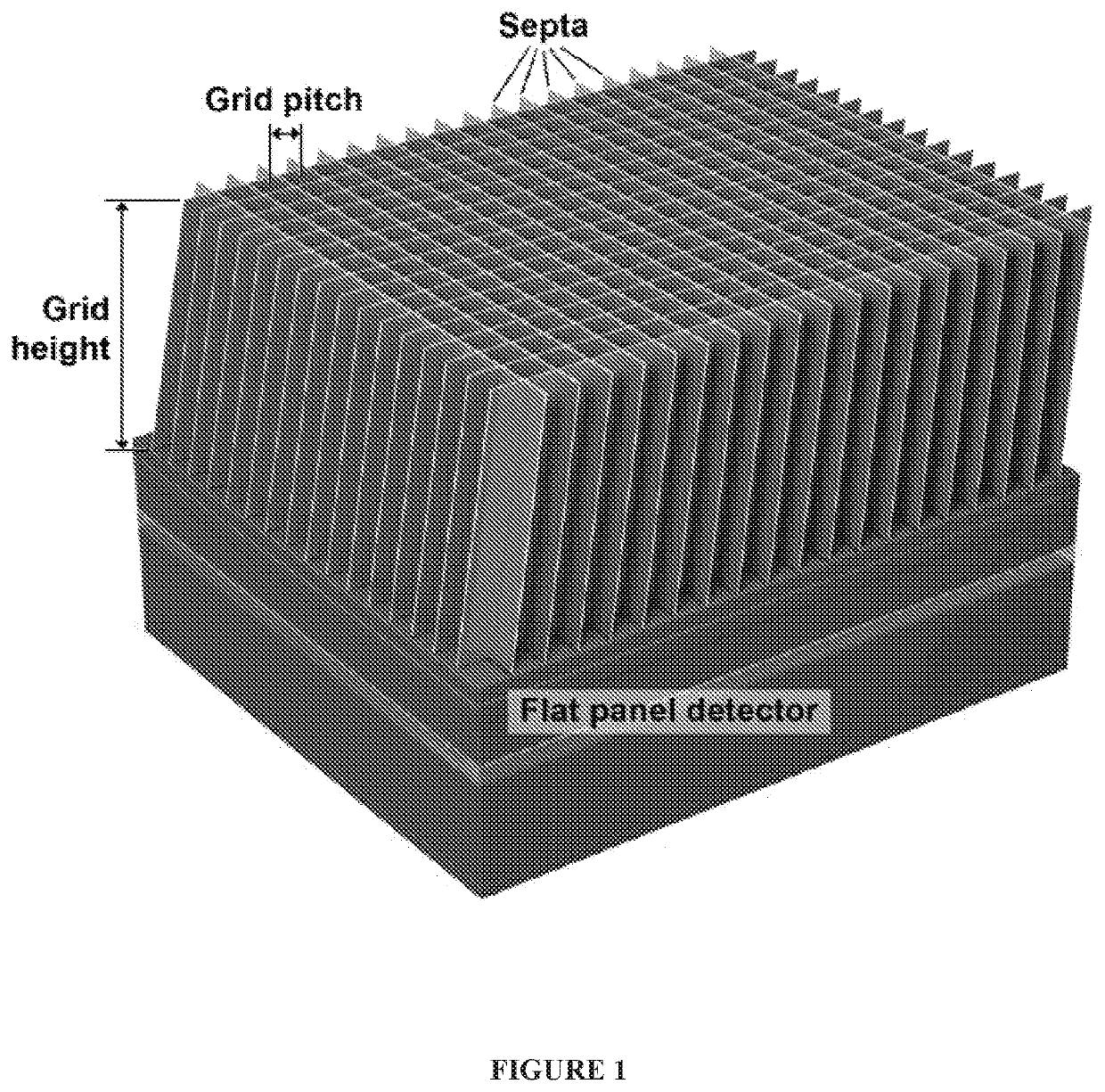
[0274]Conventional, Potter-Bucky Antiscatter Grid:

[0275]An array of 1D lead strips and inter-spacers (so called Potter-Bucky grids). Such Potter-Bucky grids absorb scattered x-rays while transmitting primary x-rays. Such grids are an “add-on” component to the flat panel detector assembly.

[0276]Phosphor (Scintillator Layer):

[0277]Phosphor layer absorbs incident x-rays and converts them to visible light photons. It is a continuous layer placed (or directly deposited) on the detector's pixel array. Since phosphor is a continuous layer, visible light photons from an x-ray interaction, diffuse within the phosphor, and spread over to multiple pixels. Thus it reduces the spatial resolution of the detector.

[0278]Detector Pixel Array:

[0279]It converts the visible light photons to electrical charge, which is converted to digitized signal.

[0280]One of the disadvantages of this approach the increased distance between the pixel array...


PUM


Abstract

The present invention relates generally to X-ray detectors and more particularly to a system and a method for integrating an anti-scattering grid with scintillators to significantly enhance the performance of flat panel X-ray detector. In particular, the performance of a flat panel X-ray detector may be enhanced by photon counting detector pixels configured underneath the septa of a 2D antiscatter grid.

Description

CROSS-REFERENCE TO RELATED APPLICATIONS[0001]The present application claims the benefit of U.S. Provisional Patent Application Nos. 62 / 486,113 filed Apr. 17, 2017; 62 / 573,021 filed Oct. 16, 2017; and 62 / 576,265 filed Oct. 24, 2017, Year, which are incorporated herein by reference.STATEMENT OF GOVERNMENTAL SUPPORT[0002]This invention was made with government support under grant number R21CA198462 awarded by the National Cancer Institute of the National Institutes of Health. The government has certain rights in the invention.FIELD OF THE INVENTION[0003]The present invention relates generally to X-ray detectors and more particularly to a system and a method for integrating an anti-scattering grid with scintillators to significantly enhance the performance of flat panel X-ray detector. In particular, the performance of a flat panel X-ray detector may be enhanced by photon counting detector pixels configured underneath the septa of a 2D antiscatter grid.BACKGROUND OF THE INVENTION[0004]T...

Claims


Application Information

Patent Timeline
Patent Type & Authority Applications(United States)
IPC IPC(8): A61B6/00G01T1/20G01T7/00
CPCA61B6/4283A61B6/4035G01T1/2002A61B6/4216G01T7/00G01T1/2006A61B6/4291G01T1/00G01T1/1648G01T1/20G01T1/2985A61B6/032A61B6/4085A61B6/4233G21K1/025
Inventor ALTUNBAS, CEM
Owner UNIV OF COLORADO THE REGENTS OF
Why Eureka
Try Eureka