Thermal conductive layer, photosensitive layer, photosensitive composition, manufacturing method for thermal conductive layer, and laminate and semiconductor device

Pending Publication Date: 2021-02-11
FUJIFILM CORP
View PDF5 Cites 2 Cited by
  • Summary
  • Abstract
  • Description
  • Claims
  • Application Information

AI Technical Summary

Benefits of technology

The present invention provides a new thermal conductive layer with better thermal conductivity and electrical insulation for use in semiconductor devices. The method of manufacturing the layer ensures its effectiveness in suppressing heat-related issues in the equipment.

Problems solved by technology

However, a three-dimensional lamination integration technique capable of achieving high integration without depending on miniaturization of a transistor has been attracting attention, since physical limitations on transistor miniaturization are approaching.
As the performance of a three-dimensionally laminated LSI device (hereinafter, also referred to as “laminated LSI”) becomes higher, an increase in power consumption and the problem of heat generation due to the increased power consumption have become important issues in design technology and packaging technology.
In the laminated LSI, the heat generated from an inside LSI device cannot be appropriately dissipated by a conventional method of dissipating heat from a package surface.
Therefore, there is a concern about an increase in leak current that leads to an increase in power consumption, and a malfunction of a circuit.
Furthermore, the heat has various adverse effects not only on the laminated LSI itself, but also on the electronic equipment incorporating the same.

Method used

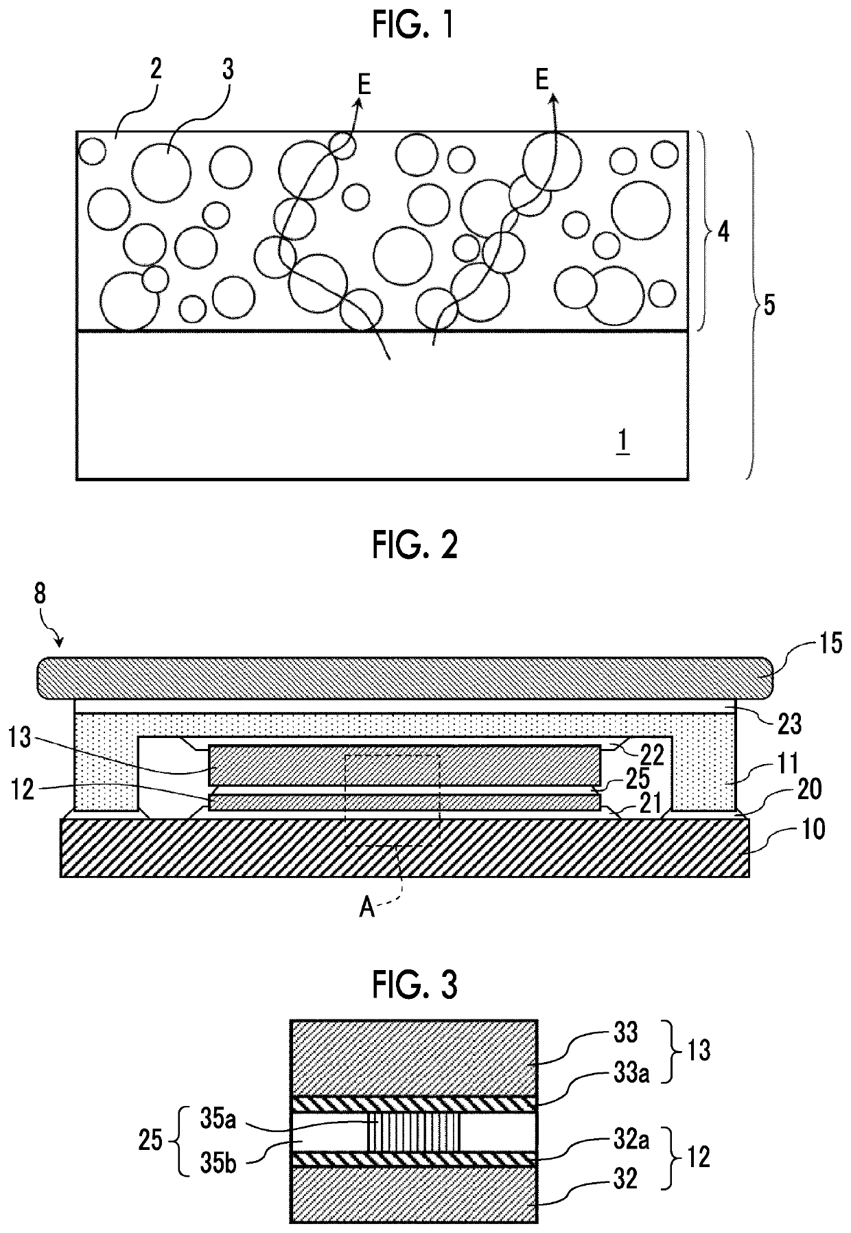
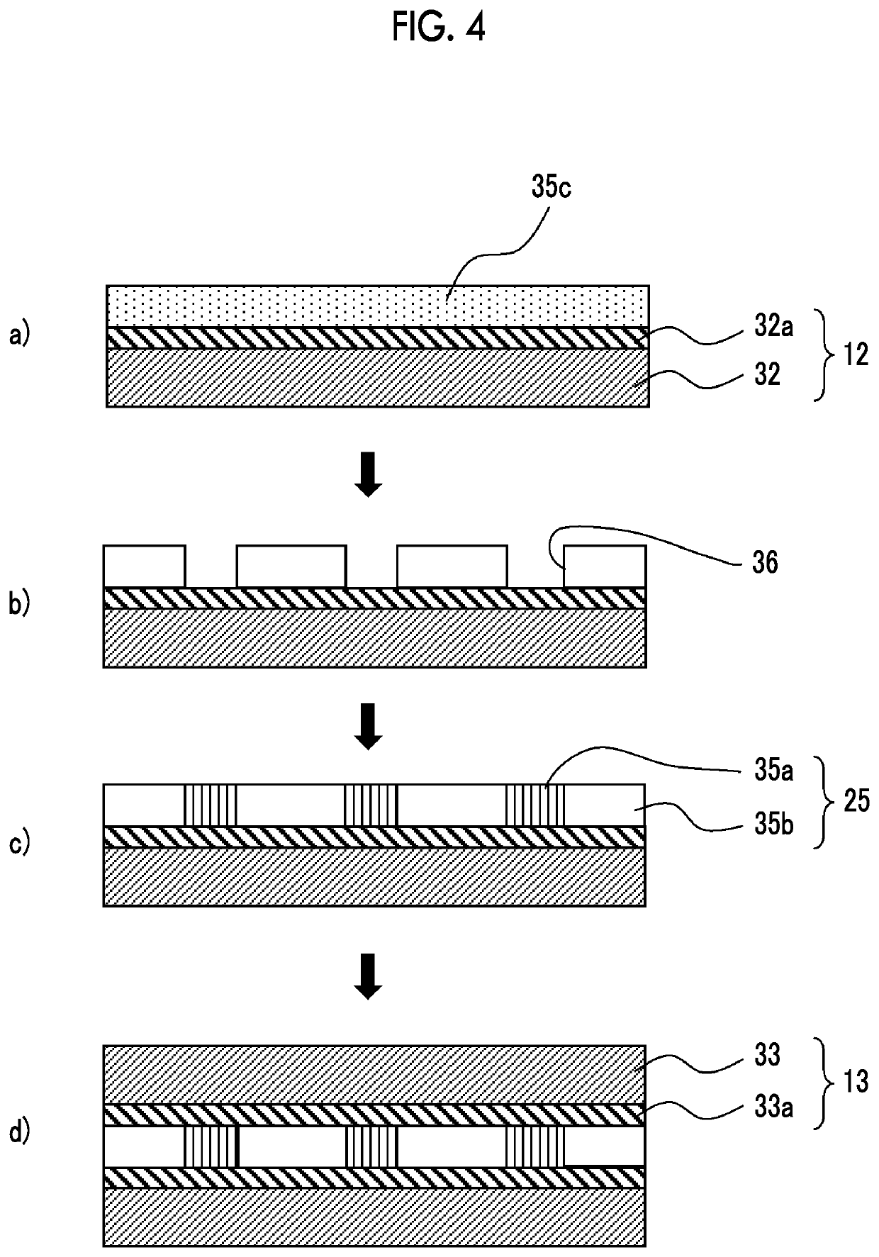

Image

  • Thermal conductive layer, photosensitive layer, photosensitive composition, manufacturing method for thermal conductive layer, and laminate and semiconductor device
  • Thermal conductive layer, photosensitive layer, photosensitive composition, manufacturing method for thermal conductive layer, and laminate and semiconductor device
  • Thermal conductive layer, photosensitive layer, photosensitive composition, manufacturing method for thermal conductive layer, and laminate and semiconductor device

Examples


examples

[0452]Hereinafter, the present invention will be described more specifically with reference to examples. The materials, used amounts, ratios, treatment contents, treatment procedures, and the like shown in the following examples can be appropriately changed without departing from the spirit of the present invention. Therefore, the scope of the present invention is not limited to the specific examples shown below. “Parts” and “%” are based on mass unless otherwise specified.

[0453]In addition, in the following examples, the weight-average molecular weight (Mw) and the number-average molecular weight (Mn) are each defined as a value in terms of polystyrene measured by gel permeation chromatography (GPC). For example, the weight-average molecular weight (Mw) and number-average molecular weight (Mn) in the examples can be determined using HLC-8220 (manufactured by Tosoh Corporation), and using TSKgeI Super AWM-H (manufactured by Tosoh Corporation, 6.0 mm (inner diameter)×15.0 cm) as a co...


PUM

PropertyMeasurementUnit
Fractionaaaaaaaaaa
Fractionaaaaaaaaaa
Percent by massaaaaaaaaaa

Abstract

The present invention relates to a thermal conductive layer that includes at least one filler, has a thermal diffusivity of 5.0×10⁻⁷ m2 s−1 or more, and has a volume resistivity of 1.0×10¹¹ Ω·cm or more. Further, the present invention relates to a photosensitive layer to which the thermal conductive layer is applied, a photosensitive composition, a manufacturing method for a thermal conductive layer, and a laminate and a semiconductor device.

Description

CROSS-REFERENCE TO RELATED APPLICATIONS[0001]This application is a Continuation of PCT International Application No. PCT / JP2019 / 016086 filed on Apr. 15, 2019, which claims priority under 35 U.S.C. § 119(a) to Japanese Patent Application No. 2018-081904 filed on Apr. 20, 2018, Japanese Patent Application No. 2018-185069 filed on Sep. 28, 2018 and Japanese Patent Application No. 2019-041304 filed on Mar. 7, 2019. Each of the above application(s) is hereby expressly incorporated by reference, in its entirety, into the present application.BACKGROUND OF THE INVENTION1. Field of the Invention[0002]The present invention relates to a thermal conductive layer which is used in electronic equipment such as a semiconductor device. Further, the present invention relates to a photosensitive layer for forming the thermal conductive layer, a manufacturing method for the thermal conductive layer, a laminate having the thermal conductive layer or the photosensitive layer, and a semiconductor device.2...

Claims


Application Information

Patent Timeline
IPC IPC(8): C09K5/14C08K3/38C08K3/22C08K3/34C08K3/04C08K9/02C08K3/28C08K7/04H01L23/373
CPCC09K5/14G03F7/322C08K3/22C08K3/34C08K3/042C08K9/02C08K3/28C08K7/04H01L23/3737C08K2201/001C08K2003/385C08K2003/282C08K2003/2241C08K2003/2227C08K2201/005C08K2201/016C08K3/38C08L33/04C08L63/00C08L79/08C08L101/00H01L2224/33181G03F7/0047G03F7/325G03F7/0388G03F7/027G03F7/033G03F7/0755G03F7/038H01L23/42C08K3/013C08L33/00C08L101/06G03F7/004G03F7/0043G03F7/20G03F7/26
Inventor YAMASHITA, KOSUKESHIMADA, KAZUTO
Owner FUJIFILM CORP
Why Eureka
Try Eureka