Manufacturing method of low temperature poly-silicon substrate (LTPS)

a manufacturing method and low temperature technology, applied in the field of liquid crystal display, can solve the problems of long manufacturing time and high production cost of the manufacturing method, and achieve the effects of reducing manufacturing steps, optimizing the manufacturing method, and reducing the thickness of the ltps array substra

Active Publication Date: 2021-02-18
WUHAN CHINA STAR OPTOELECTRONICS TECH CO LTD
View PDF9 Cites 0 Cited by
  • Summary
  • Abstract
  • Description
  • Claims
  • Application Information

AI Technical Summary

Benefits of technology

[0030]The advantages of the present disclosure includes: when a structure of semiconductor device is not changed, the manufacturing method is optimized. The gate insulating and interlayer insulating layer is formed by one-time chemical vapor d

Problems solved by technology

Therefore, the manufacturing method of LTPS array substrate requires more film layers, the manufacturing met

Method used


Image

  • Manufacturing method of low temperature poly-silicon substrate (LTPS)
  • Manufacturing method of low temperature poly-silicon substrate (LTPS)
  • Manufacturing method of low temperature poly-silicon substrate (LTPS)

Examples


embodiment 1

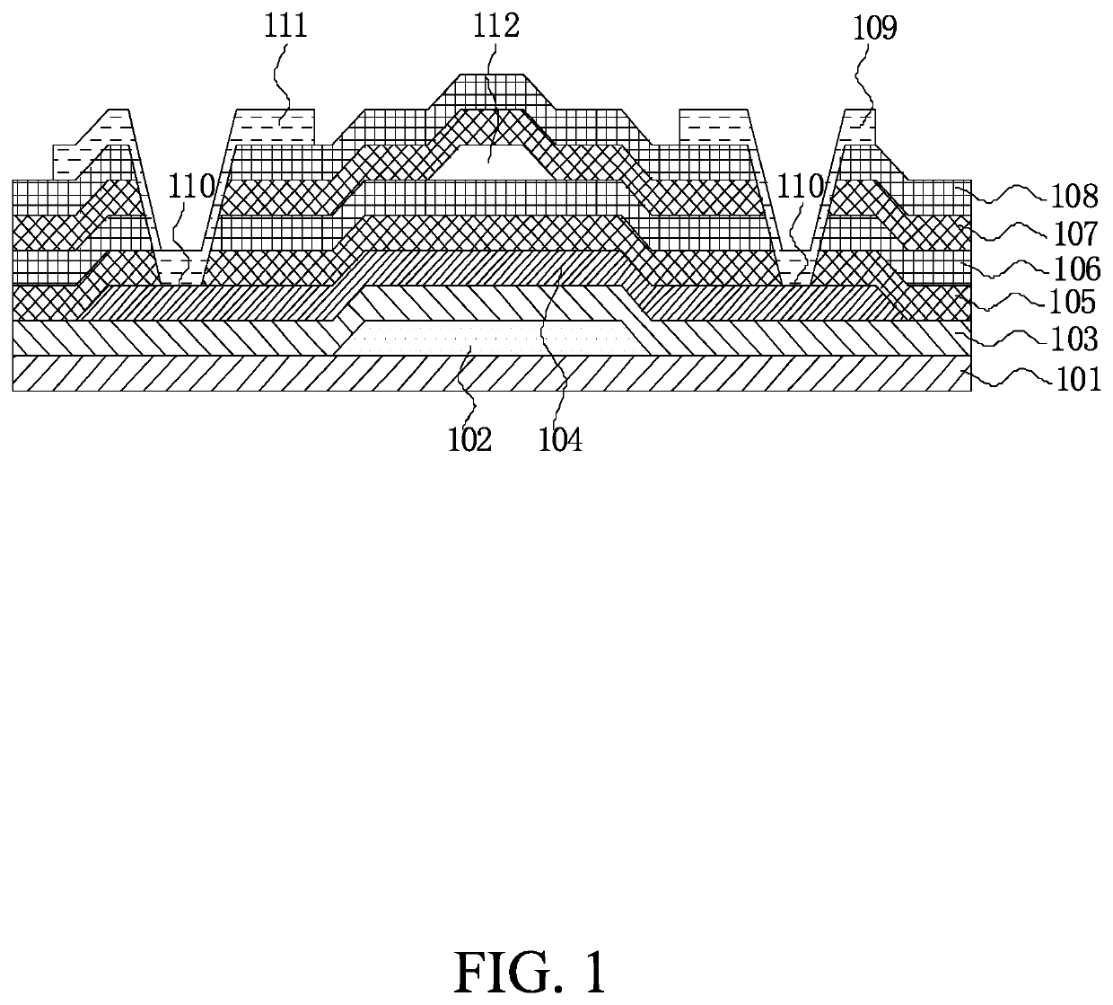
[0041]The present disclosure provides a manufacturing method of an LTPS array substrate, the manufacturing method is described in detail in conjunction with FIG. 2 to FIG. 6.

[0042]As shown in the figures, the manufacturing method includes the following steps.

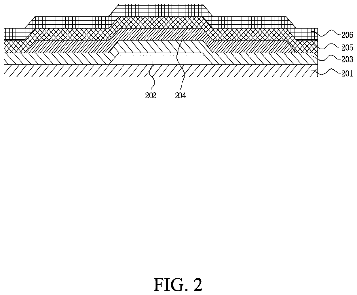
[0043]In step S10, as shown in FIG. 2, a substrate 201 is provided, the substrate 201 is made of a transparent substrate, e.g. a transparent glass substrate. A metal layer is deposited on the substrate 201, and the metal layer is patterned by a photo-etching process. A metal light-shielding layer 202 is formed on the substrate 201. A material of the metal light-shielding layer 202 includes molybdenum aluminum alloy, chromium, molybdenum, or materials with the light shielding function and electric conductivity simultaneously.

[0044]In step S20, the buffer layer 203 is formed on the metal light-shielding layer 202. A material of the buffer layer 203 includes silicon nitride, silicon oxide, or a combination of the silicon nitride an...

embodiment 2

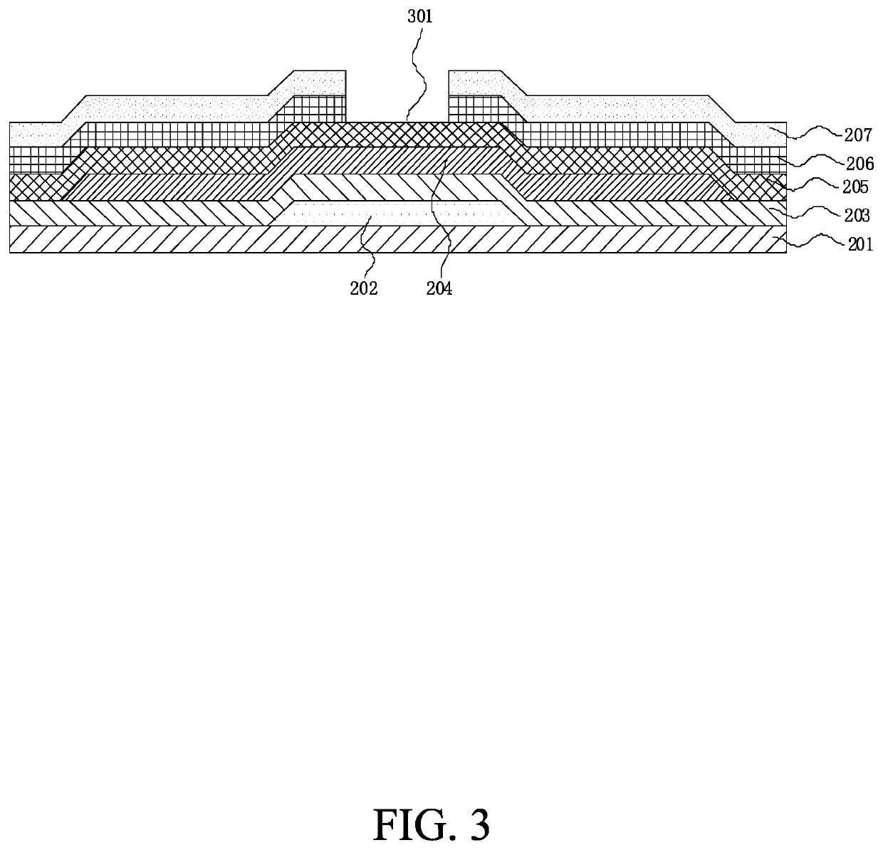
[0049]In the first embodiment, a trench for a gate line is formed in the gate insulating and interlayer insulating layer. A gate line trench is formed by the trench and a gate line is formed in the gate line trench. The gate line, the source electrode, and the drain electrode are disposed on the same layer, such that a structure of the LTPS array substrate is simplified, and the thickness of the LTPS array substrate is reduced. In contrast, the process of forming gate line trenches by exposure and etching process, and physical vapor deposition are required according to the first embodiment of the present disclosure.

[0050]As described in the embodiment of FIG. 7, the manufacturing steps of gate line trenches are omitted. After the steps S10 to S40 are performed as described in the first embodiment, a polycrystalline silicon layer 701, a first gate insulating and interlayer insulating layer 702, a second gate insulating and interlayer insulating layer 703 are formed. A positive photor...


PUM


Abstract

A manufacturing method of a low temperature poly-silicon (LTPS) array substrate is described. The LTPS array substrate includes a metal light-shielding layer, a buffer layer, a polycrystalline silicon layer, a gate insulating and interlayer insulating layer, a gate line layer, and a source and drain electrode layer. The method adopts a one-time chemical vapor deposition process to form a gate insulator and interlayer insulating layer. A gate line trench is formed in the gate insulating layer and the interlayer insulating layer, thereby reducing the thickness of the LTPS array substrate film layer and the process steps.

Description

BACKGROUNDField[0001]The present disclosure relates to a technical field of liquid crystal displays, and more particularly to a manufacturing method of low temperature poly-silicon array substrates (LTPS).Background[0002]In a manufacturing procedure of display screens, because product cost made of low temperature poly-silicon (LTPS) is low and the electron mobility of the device is high, display manufacturers of mobile phones and tablet screens are in favor of these products.[0003]In a conventional LTPS manufacturing process, the LTPS array substrate uses two times of chemical vapor deposition process on the polycrystalline silicon layer in the process for forming a gate insulator (GI) and an interlayer dielectric (ILD), where the gate insulating layer and the interlayer insulating film are regarded as two layer structures individually.[0004]FIG. 1 is a schematic cross-sectional structure of a low temperature poly-silicon (LTPS) array substrate in the prior art. In the structure of ...

Claims


Application Information

Patent Timeline
IPC IPC(8): H01L29/66H01L21/311H01L21/285H01L21/3213
CPCH01L29/66757H01L21/32139H01L21/2855H01L21/31116H01L27/1259H01L27/1262G02F1/1303G02F1/1362H01L27/1288H01L29/78633
Inventor CHEN, CHEN
Owner WUHAN CHINA STAR OPTOELECTRONICS TECH CO LTD
Why Eureka
Try Eureka