
Photoelectric conversion element and imaging device

a conversion element and imaging device technology, applied in the field of photoelectric conversion elements and imaging devices, can solve the problems of reducing the number of photons that enter the unit pixel, lowering the sensitivity as well as the s/n ratio, and reducing the sensitivity, so as to improve the performance, and reduce the occurrence of dark curren

Pending Publication Date: 2021-03-18
SONY SEMICON SOLUTIONS CORP
View PDF0 Cites 0 Cited by
  • Summary
  • Abstract
  • Description
  • Claims
  • Application Information

AI Technical Summary

Benefits of technology

This patent describes a photoelectric conversion element and an imaging device that can reduce dark current, which is an unwanted electrical current. By using an organic semiconductor material for the photoelectric conversion layer, the element can better match the energy levels of other materials in the layer. This results in a more effective conversion of light into electricity, while minimizing dark current. Overall, the technology improves image quality by reducing dark current and other distortions.

Problems solved by technology

This leads to a decrease in the number of photons that enter a unit pixel, thus leading to lowered sensitivity as well as a lowered S / N ratio.
Further, in a case of using a color filter in which primary color filters of red, green, and blue are two-dimensionally arrayed for colorization, beams of light of green and blue are absorbed by the color filter in a red pixel, thus leading to lowered sensitivity.
Furthermore, interpolation processing is performed between pixels upon generation of each color signal, thus causing occurrence of a so-called false color.

Method used


Image

  • Photoelectric conversion element and imaging device
  • Photoelectric conversion element and imaging device
  • Photoelectric conversion element and imaging device

Examples


embodiment

1. EMBODIMENT

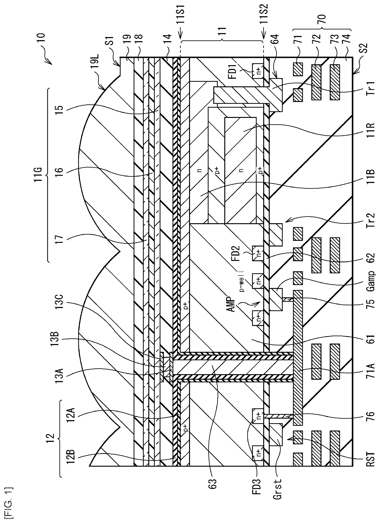
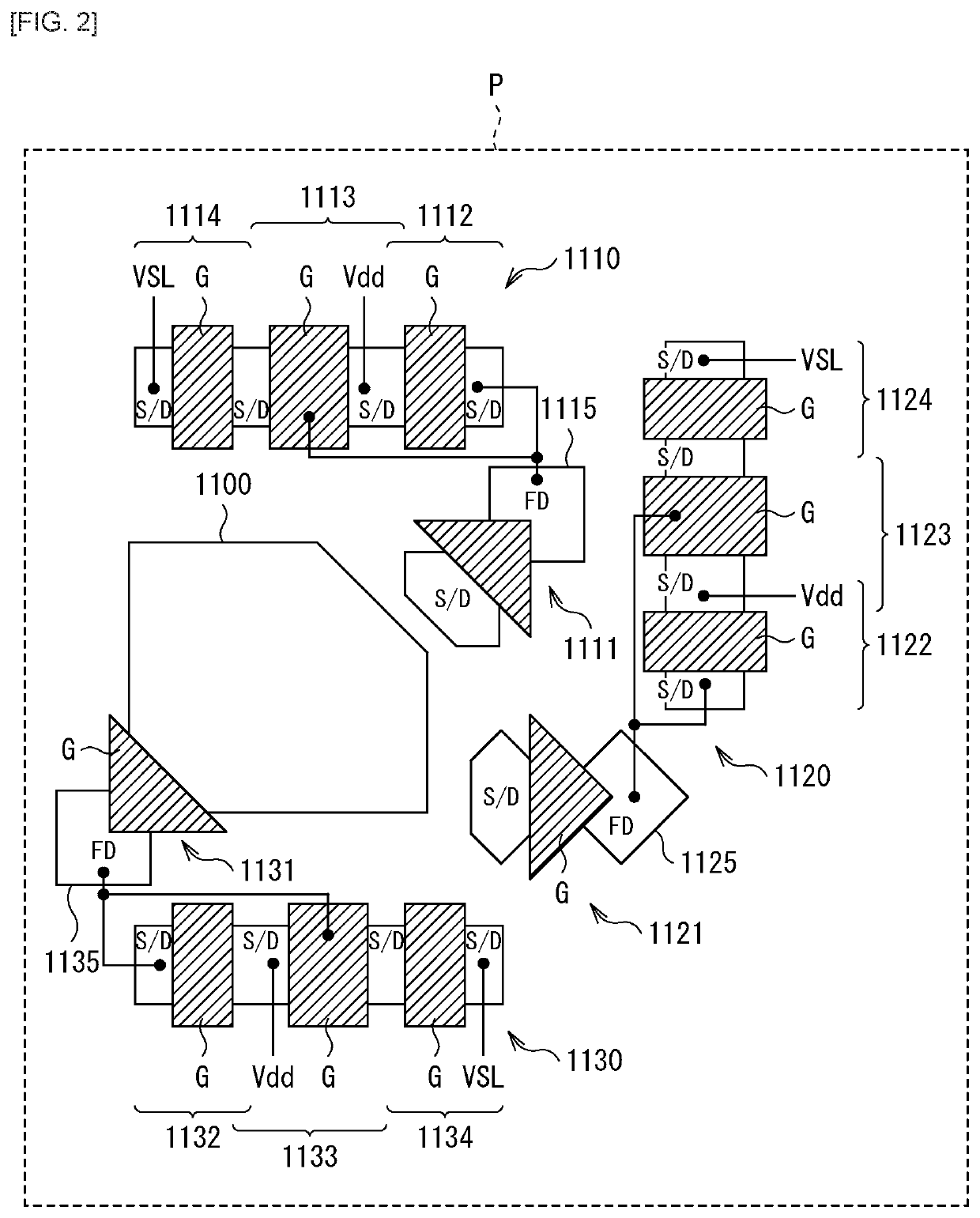
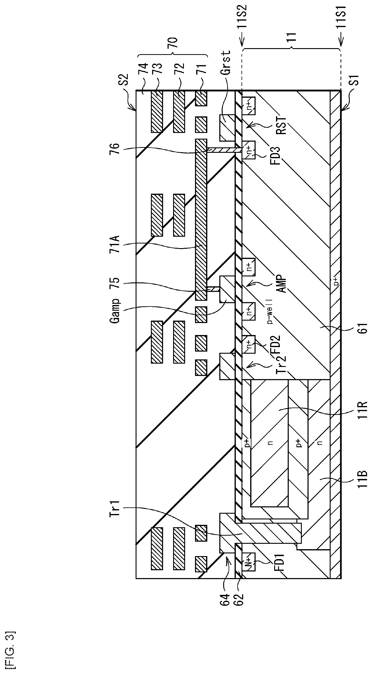
[0038]FIG. 1 illustrates a cross-sectional configuration of a photoelectric conversion element (a photoelectric conversion element 10) according to an embodiment of the present disclosure. The photoelectric conversion element 10 is used, for example, as an imaging element that configures one pixel (a unit pixel P) in an imaging device (an imaging device 1) such as a backside illumination type (backside light receiving type) CCD (Charge Coupled Device) image sensor or a CMOS (Complementary Metal Oxide Semiconductor) image sensor (see FIG. 5). The photoelectric conversion element 10 is of a so-called vertical spectroscopic type in which one organic photoelectric conversion section 11G and two inorganic photoelectric conversion sections 11B and 11R that selectively detect light in different wavelength regions to perform photoelectric conversion are stacked in a vertical direction. In the present embodiment, an organic photoelectric conversion layer 16 that configures an or...

application examples

2. APPLICATION EXAMPLES

Application Example 1

[0119]FIG. 5 illustrates, for example, an overall configuration of the imaging device 1 in which the photoelectric conversion element 10 described in the foregoing embodiment is used for each pixel. The imaging device 1 is a CMOS imaging sensor. The imaging device 1 has a pixel section 1a as an imaging area on the semiconductor substrate 11, and includes, for example, a peripheral circuit section 130 configured by a row scanning section 131, a horizontal selection section 133, a column scanning section 134, and a system control section 132 in a peripheral region of the pixel section 1a.

[0120]The pixel section 1a includes, for example, a plurality of unit pixels P (corresponding to, e.g., photoelectric conversion elements 10) arranged two-dimensionally in matrix. To the unit pixels P, for example, pixel drive lines Lread (specifically, row selection lines and reset control lines) are wired on a pixel-row basis, and vertical signal lines Ls...

application example 2

[0125]The above-described imaging device 1 is applicable to any type of electronic apparatus (imaging device) having an imaging function, for example, a camera system such as a digital still camera and a video camera, and a mobile phone having the imaging function. FIG. 6 illustrates an outline configuration of a camera 2 as an example thereof. This camera 2 is, for example, a video camera that is able to photograph a still image or shoot a moving image. The camera 2 includes, for example, the imaging device 1, an optical system (optical lens) 310, a shutter device 311, a drive section 313 that drives the imaging device 1 and the shutter device 311, and a signal processing section 312.

[0126]The optical system 310 guides image light (incident light) from a subject to the pixel section 1a in the imaging device 1. The optical system 310 may be configured by a plurality of optical lenses. The shutter device 311 controls periods of light irradiation and light shielding with respect to th...


PUM

PropertyMeasurementUnit
HOMO levelaaaaaaaaaa
wavelength bandaaaaaaaaaa

Abstract

A photoelectric conversion element according to an embodiment of the present disclosure includes: a first electrode; a second electrode disposed to be opposed to the first electrode; and a photoelectric conversion layer provided between the first electrode and the second electrode and including an organic semiconductor material represented by the following general formula (1), in which the organic semiconductor material includes, in at least one of R2 or R6, a substituent represented by the following general formula (2).

Description

TECHNICAL FIELD[0001]The present disclosure relates to a photoelectric conversion element using an organic semiconductor and an imaging device including the photoelectric conversion element.BACKGROUND ART[0002]In recent years, there has been progress in reduction of a pixel size in a solid-state imaging device such as a CCD (Charge Coupled Device) image sensor or a CMOS (Complementary Metal Oxide Semiconductor) image sensor. This leads to a decrease in the number of photons that enter a unit pixel, thus leading to lowered sensitivity as well as a lowered S / N ratio. Further, in a case of using a color filter in which primary color filters of red, green, and blue are two-dimensionally arrayed for colorization, beams of light of green and blue are absorbed by the color filter in a red pixel, thus leading to lowered sensitivity. Furthermore, interpolation processing is performed between pixels upon generation of each color signal, thus causing occurrence of a so-called false color.[0003...

Claims


Application Information

Patent Timeline
Patent Type & Authority Applications(United States)
IPC IPC(8): H01L27/30H01L51/42H01L51/00
CPCH01L27/307H01L51/4213H01L51/0052H01L51/0078H01L51/0074H01L51/0047H01L51/008H01L51/0067H01L51/0046H01L27/146Y02E10/549H10K39/32H10K85/615H10K85/322H10K30/10H10K85/211H10K85/215H10K85/311H10K85/654H10K85/6576
Inventor ENOKI, OSAMUHASEGAWA, YUTANEGISHI, YUKIYAGI, IWAOUJIIE, YASUHARUSAITO, YOSUKE
Owner SONY SEMICON SOLUTIONS CORP
Learn More