Thermal management package and method

a technology of thermal management package and package, which is applied in the direction of semiconductor devices, semiconductor/solid-state device details, electrical apparatus, etc., can solve the problems of reducing the efficiency of solid-state power devices, and increasing the cost of embedding process, so as to achieve high thermal conductivity, reduce the cost, and eliminate the effect of cracks

Active Publication Date: 2021-07-08
MICROCHIP TECH INC
View PDF0 Cites 1 Cited by
  • Summary
  • Abstract
  • Description
  • Claims
  • Application Information

AI Technical Summary

Benefits of technology

[0012]The present invention is directed to a thermal management package employing embedded high thermal conductivity material, such as a metal in the form of a slug, enhanced by disposing it within a first window in a high dielectric constant material substrate disposed within a second window in a low dielectric constant outer substrate that provides a smaller and therefo

Problems solved by technology

One problem that needs to be addressed is that solid-state power devices are presently limited in their ability to generate kilowatts of power in a light weight and small size, lower-cost packaging.
Another issue that must be managed in packaging RF power semiconductor devices is RF impedance matching between the RF power semiconductor devices and the circuitry to which they are coupled.
The embedding process adds to the cost.
This technology has a relatively large footprint and adds significant weight.
The use of metal slugs in such relatively large footprint high dielectric constant laminate circuit board materials is prone to cracking around the slug

Method used


Image

  • Thermal management package and method
  • Thermal management package and method
  • Thermal management package and method

Examples


Embodiment Construction

[0042]Persons of ordinary skill in the art will realize that the following description is illustrative only and not in any way limiting. Other embodiments will readily suggest themselves to such skilled persons.

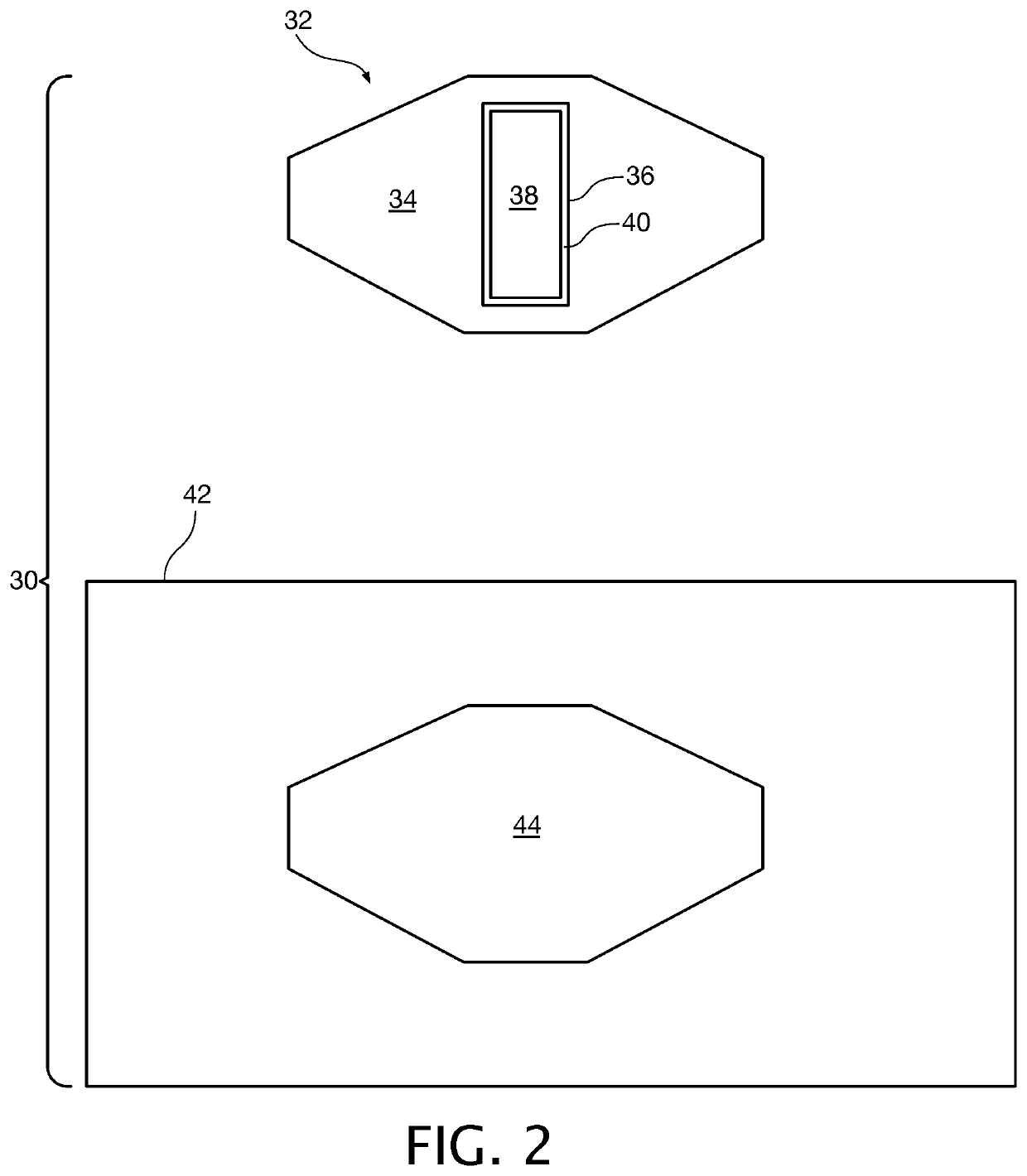
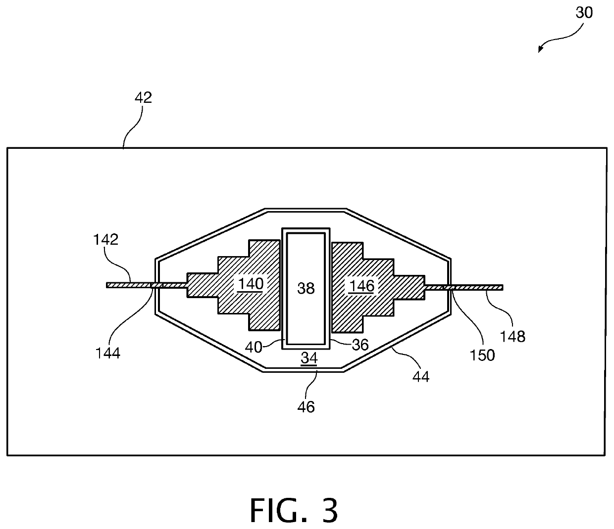
[0043]Referring first of all to FIG. 2 and FIG. 3, which show top views show a thermal management package 30 in accordance with an aspect of the present invention. The thermal management package 30 has a semiconductor mount sub-assembly 32 formed from a high dielectric constant material substrate 34 including a first window 36 into which a high thermal conductivity slug 38 is bonded using a bonding material shown at reference numeral 40. The dielectric constant is synonymous with relative permittivity, is denoted εr, and is a function of frequency. For the purposes of this document, the frequency of interest is the frequency at which the high dielectric constant material substrate 34 exhibits the lowest dielectric constant over the operating frequency of the semiconductor dev...


PUM


Abstract

A thermal management package for a semiconductor device includes a high dielectric constant material substrate, a high thermal conductivity slug disposed in a first window in the high dielectric constant material substrate and held therein by a first bonding material, an outer substrate formed from a material having a low dielectric constant and having a second window formed therein, the high dielectric constant material substrate disposed in the second window in the low dielectric constant outer substrate and held therein by a second bonding material.

Description

[0001]The present invention relates to semiconductor mounting structures. More particularly, the present invention relates to an embedded high thermal conductivity slug held within a high dielectric constant material substrate that is placed within a window in a low dielectric constant outer substrate.BACKGROUND[0002]The ultimate goal of high-power radio frequency (RF) semiconductor technology, especially GaN semiconductor technology is to replace vacuum-tube based power solutions at all frequencies. One problem that needs to be addressed is that solid-state power devices are presently limited in their ability to generate kilowatts of power in a light weight and small size, lower-cost packaging. What is needed is smaller and more capable power devices coupled with smaller and more capable pallet / module solutions to improve thermal management, reduce the size, weight and lower the cost of the solution.[0003]FIGS. 1A through 1D are diagrams showing cross sectional views of semiconduct...

Claims


Application Information

Patent Timeline
IPC IPC(8): H01L23/367H01L23/373
CPCH01L23/367H01L23/3735H01L23/3732H01L23/3677H01L23/66H01L2223/6655H01L2223/6683H01L24/10H01L25/16H01L25/18H01L23/3736H01L23/3731H01L2224/48091H01L2224/16225H01L2224/73265H01L2224/48227H01L2924/181H01L2924/00014H01L24/14H01L2224/1403H01L2224/1703H01L24/17H01L24/73H01L24/16H01L24/48H01L2924/00012H01L2224/45099
Inventor MCCANN, DAMIAN
Owner MICROCHIP TECH INC
Why Eureka
Try Eureka