High-Flux Filter Membrane with Three-Dimensional and Self-Aligned Micropores Arrays and Method for Manufacturing Same
a filter membrane and high-flux technology, applied in membrane technology, membrane materials, chemistry apparatuses and processes, etc., can solve the problems of easy blockage of pores, lower filtration efficiency, and increased requirements for new filter membrane types, so as to increase the fluid flux, reduce the thickness of upper pores, and increase the pore diameter of lower pores.
- Summary
- Abstract
- Description
- Claims
- Application Information
AI Technical Summary
Benefits of technology
Problems solved by technology
Method used
Image
Examples
embodiment 1
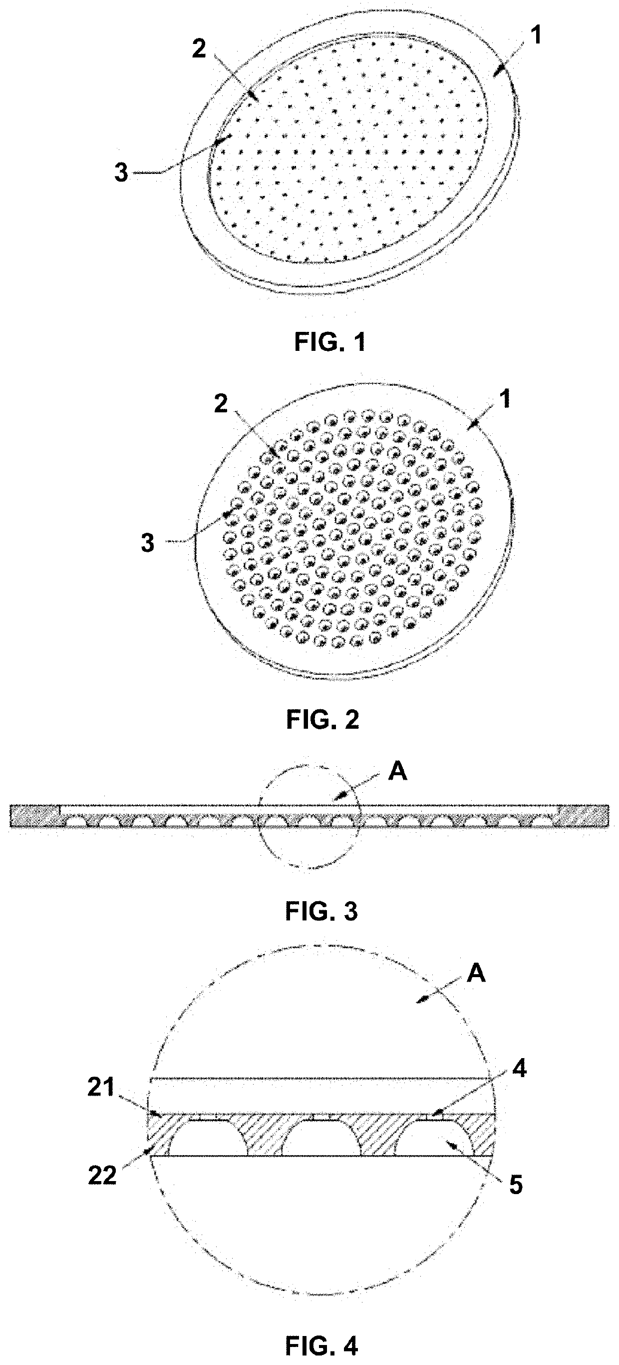
[0033]As shown in FIG. 1 to FIG. 4, a high-flux filter membrane with three-dimensional and self-aligned micropores arrays, comprises: an operating area 1, wherein the operating area 1 is located around the filter membrane; a filter area 2, wherein the filter area 2 is located in the middle of the filter membrane and relatively concave to the operating area 1; and three-dimensional and self-aligned micropores 3; wherein three-dimensional and self-aligned micropores 3 are provided on the filter area 2 and comprise upper pores 4 and lower pores 5; the upper pores 4 and the lower pores 5 are coaxial pores; the upper pores 4 are cylindrical poreswith diameter is less than that of the lower pores 5; the upper pores 4 connect with the lower pores 5; the fluid sequentially flows through the upper pores 4 and the lower pores 5; the lower pores 5 are conical pores whose pore diameter gradually increases from top to bottom.
[0034]The filter membrane is circular with diameter ranges from 1 mm to...
embodiment 2
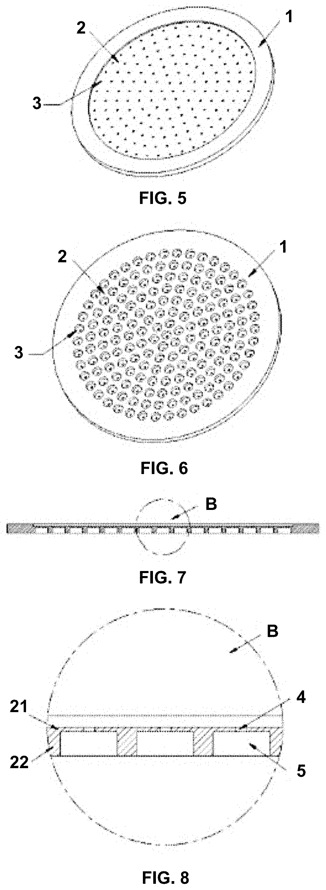
[0037]As shown in FIG. 5 to FIG. 8, based on Embodiment 1, the lower pores 5 are cylindrical pores with diameter ranging from 1.1 μm to 50 μm.
embodiment 3
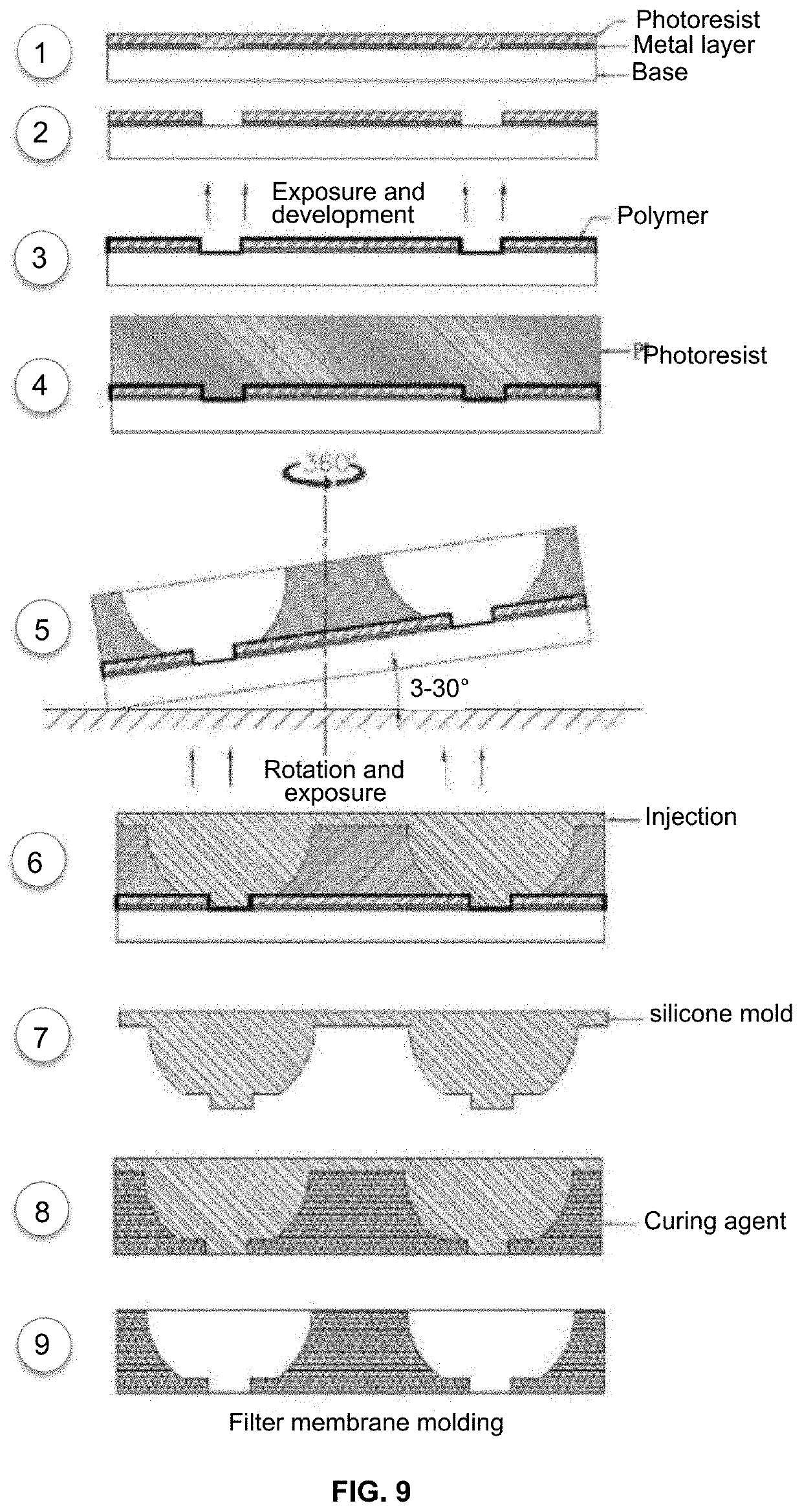
[0038]A method for manufacturing a high-flux filter membrane with three-dimensional and self-aligned micropores arrays, comprises: coating a metal layer (e.g. chromium, gold, and the like) on an optical template (base); forming a microporous structure on the metal layer; spin-coating a photoresist on the metal layer, back-side exposing and developing; depositing a polymer on the photoresist after development; spin-coating the photoresist on the polymer again, shifting upward by 30°, rotating, back-side overexposing, normally developing, and replicating using a soft photolithography method to obtain a silicone mold (as shown in FIG. 10); and imprinting the silicone mold using an lithography technology to obtain the microporous filter membrane.
[0039]The polymer is parylene with a deposition thickness ranging from 10 nm to 500 nm.
[0040]FIG. 11 is an scanning electronic microscope of the surface of the microporous filter membrane manufactured in the present application. As shown in FIG....
PUM
| Property | Measurement | Unit |
|---|---|---|
| thickness | aaaaa | aaaaa |
| thickness | aaaaa | aaaaa |
| diameter | aaaaa | aaaaa |
Abstract
Description
Claims
Application Information


