Element manufacturing method

Pending Publication Date: 2021-12-02
ENECOAT TECH CO LTD
View PDF0 Cites 0 Cited by
  • Summary
  • Abstract
  • Description
  • Claims
  • Application Information

AI Technical Summary

Benefits of technology

[0026]An invention described in this specification provides a method for manufacturing an element which does not lead to the occurrence of a short due to etching. Further, an invention described in this specification provides a method for manu

Problems solved by technology

However, if such etching is performed, the portion that is masked is also removed, and this has caused a short (short circuit).
In particular, when separating the power generation layer by dry etching using plasma generated by a carbon tetrafluoride

Method used


Image

  • Element manufacturing method
  • Element manufacturing method
  • Element manufacturing method

Examples


Example

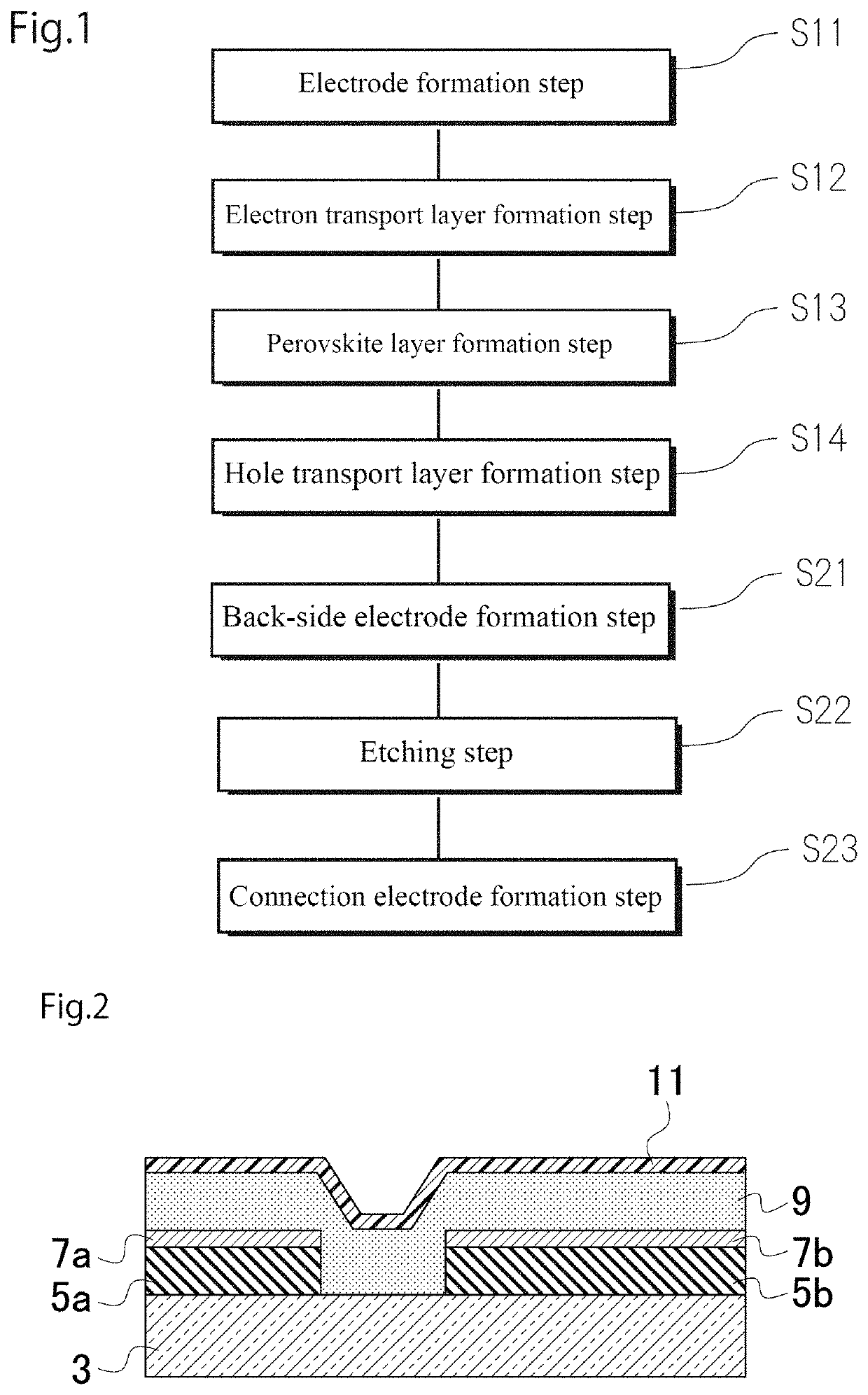
[0096]FIG. 9 is a schematic view for explaining a solar cell according to Embodiment 1.

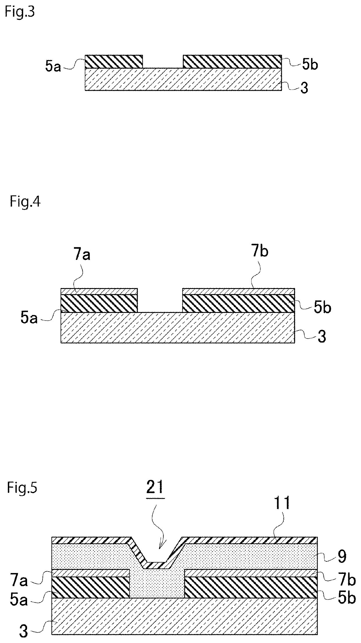
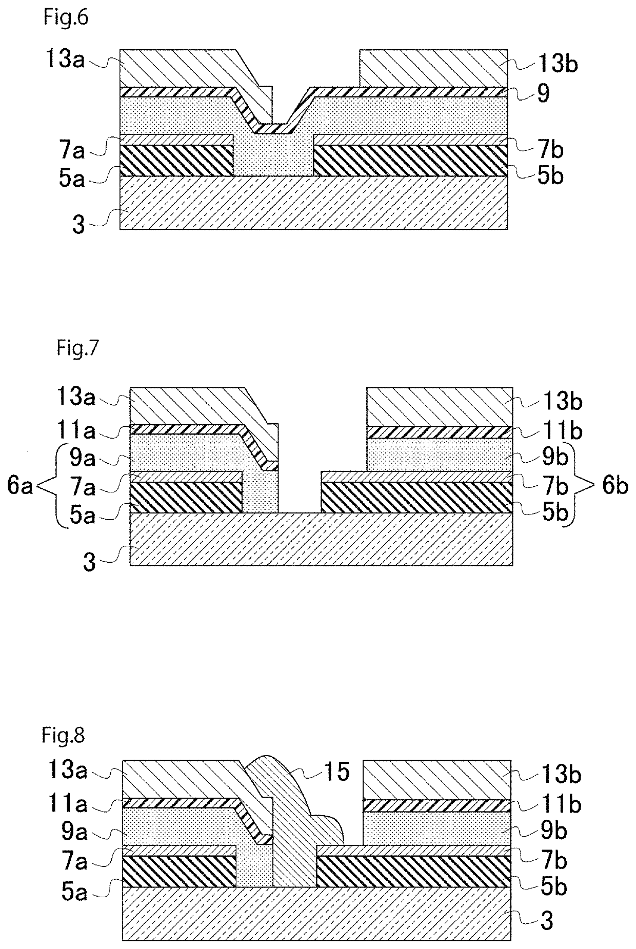
[0097]On a glass substrate 3, there is an ITO (indium tin oxide) of the electrode 5 that has been patterned into a prescribed shape in advance. Thereon, the electron transport layer 7, the perovskite layer 9, and the hole transport layer 11 are sequentially applied. The electron transport layer 7 can be formed by spin coating and then drying a colloidal SnO2 aqueous solution. The perovskite layer 9 can be obtained with high quality by applying a prescribed material by spin coating and then further coating a poor solvent. The hole transport layer 11 can be obtained by spin coating and then drying a solution containing Spiro-MeOTAD.

[0098]The above layers are formed based on spin coating, and thus they are laminated over the entire surface of the substrate.

[0099]In the prior art, it was common to perform a process of patterning the layers that were laminated before the formation of the back-side elec...

Example

[0105]In Embodiment 2 shown in FIG. 10(a), connection regions of the back-side electrodes are provided in adjacent center regions of the surface electrodes and then connected to each other. In Embodiment 3 shown in FIG. 10(b), connection regions of the back-side electrodes are provided in adjacent regions of the surface electrodes and then connected to each other.

INDUSTRIAL APPLICABILITY

[0106]The present invention can be utilized in the technical field related to solar cells and organic EL elements.

REFERENCE SIGNS LIST

[0107]1: element[0108]3: substrate[0109]5: electrode[0110]6a: first photoelectric conversion layer[0111]6b: second photoelectric conversion layer[0112]7a: first electron transport layer[0113]7b: second electron transport layer[0114]9: perovskite layer[0115]11: hole transport layer[0116]13a: first back-side electrode[0117]13b: second back-side electrode[0118]15: connection electrode[0119]21: element material[0120]23: sealing material layer


PUM


Abstract

[Problem] To provide a method for manufacturing an element which does not lead to the occurrence of a short due to etching, and which suppresses the deterioration of a photoelectric conversion layer. [Solution] An element manufacturing method, wherein the method includes the following steps which are performed on an element material including an electrode formed on a substrate, the electrode having a first electrode and a second electrode which are separated from each other, and a photoelectric conversion layer formed in a region that includes the first electrode and the second electrode: a step in which a first back-side electrode and a second back-side electrode are formed at positions on the photoelectric conversion layer corresponding to a first electrode and a second electrode, wherein the first back-side electrode and the second back-side electrode are not connected; a step in which etching is performed using the first back-side electrode and the second back-side electrode as a mask; and a connection electrode formation step in which a connection electrode for connecting the first back-side electrode and the second back-side electrode is formed.

Description

TECHNICAL FIELD[0001]The present invention relates to a method for manufacturing an element such as a solar cell or an organic EL.BACKGROUND ART[0002]JP2018-163938A discloses a solar cell.[0003]For example, in order to obtain a solar cell module with a high voltage, it is preferable to connect cells in series within the same substrate to create a solar cell module having an integrated structure.[0004]Further, when separating a power generation layer in order to obtain a module having an integrated structure, it has been contemplated to perform etching using a mask so as to remove a portion of a perovskite layer and a hole transport layer. However, if such etching is performed, the portion that is masked is also removed, and this has caused a short (short circuit).[0005]In particular, when separating the power generation layer by dry etching using plasma generated by a carbon tetrafluoride gas and an oxygen gas, there has been a problem in that sneaking under the mask occurred, which...

Claims


Application Information

Patent Timeline
IPC IPC(8): H01G9/20H01L51/00H01L51/44
CPCH01G9/20H01L51/441H01L51/0017H10K71/60H10K85/30H10K30/81H10K30/00Y02E10/549H01L31/0463H01L31/0465Y02P70/50H10K71/231H10K30/211H10K85/50
Inventor TAKAHAMA, TSUYOSHIYABUMOTO, TOSHIHIKO
Owner ENECOAT TECH CO LTD
Why Eureka
Try Eureka