Methods of fabricating synthetic diamond materials using microwave plasma activated chemical vapour deposition techniques and products obtained using said methods

a technology of plasma active and synthetic diamond, which is applied in the direction of polycrystalline material growth, crystal growth process, chemically reactive gas growth, etc., can solve the problems of difficult to even approach the level of perfection, all diamond materials contain a significant number of defects, and the theoretical perfect diamond lattice is impossible to achieve, etc., to achieve high and uniform power density, reduce impurities, and high volume growth rate

Pending Publication Date: 2021-12-23
ELEMENT SIX TECH LTD +1
View PDF0 Cites 1 Cited by
  • Summary
  • Abstract
  • Description
  • Claims
  • Application Information

AI Technical Summary

Benefits of technology

[0035]Following on from the work described in the aforementioned documents, the present applicant has found that using suitable microwave plasma activated CVD reactor hardware and CVD diamond synthesis methodology it is possible to achieve high and uniform power densities over large substrate areas and maintain such power densities over long operating times to achieve the fabrication of large volumes of synthetic diamond material at high volume growth rates and with reduced impurities.

Problems solved by technology

Such a theoretically perfect diamond lattice is thermodynamically impossible to attain.
In reality, it is practically difficult to even approach a level of perfection which would be possible to achieve in theory when taking into account thermodynamic considerations.
As such, it should be apparent that all diamond materials contain a significant number of defects.
Such defects may come in the form of impurities.
Additionally, defects within diamond materials also include crystallographic deviations from the perfect diamond lattice structure in the form of point defects such as vacancies and interstitials and extended defects such as various forms of dislocation defects.
Defects within diamond materials significantly alter the properties of the materials.
Furthermore, the nature of the substrate material and the growth conditions affect the type and distribution of defects incorporated into the CVD synthetic diamond material during growth.
However, in such applications impurities can interact with quantum spin defects within the diamond lattice structure reducing their decoherence time and thus reducing their sensitivity and / or reducing the time during which quantum processing applications can be performed.
Nitrogen is one of the most important dopants in CVD diamond material synthesis as it has been found that providing nitrogen in the CVD process gas increases the growth rate of the material and can also affect the formation of crystallographic defects such as dislocations.
A problem with synthesizing low defect, high purity single crystal CVD synthetic diamond material is that such material has a very low growth rate and is thus time consuming and expensive to manufacture.
Furthermore, due to the extended time periods required to obtain a desired thickness of such material at low growth rates, the growth process must be very precisely controlled over extended time periods and this can be difficult to achieve in practice resulting in reduced yields.
However, while single crystal CVD synthetic diamond material according to this process is suitable for many optical applications, the concentration of nitrogen incorporated into the material is such that the material is not ideally suited for certain high-end optical applications and certain other applications such as electronic, radiation detector, and quantum sensing and processing applications which require higher purity material and a CVD growth process in which nitrogen is essentially excluded.
Furthermore, even for applications which are not detrimentally affected by the presence of a low and controlled concentration of nitrogen in the single crystal CVD synthetic diamond material, it can be difficult to obtain consistent and reproducible optical properties, such as low absorption, utilizing a low and controlled nitrogen addition.
However, such a plasma focussing route is not suitable for achieving high power densities across relatively large growth areas to enhance volume growth rate.
However, as the growth area is increased the power density decreases thus decreasing the growth rate on each individual single crystal diamond substrate.
A decrease in power density also leads to a decrease in the quality of single crystal CVD diamond material which is synthesized.
One problem with prior art methodologies is how to achieve very high purity single crystal CVD synthetic diamond material, suitable for certain high-end optical applications and certain other applications such as electronic, radiation detector, and quantum sensing and processing applications, at increased volume growth rates (e.g. over a plurality of single crystal diamond growth substrates) while avoiding the addition of nitrogen to enhance growth rates.
However, due to the polycrystalline nature of such wafers their functional properties are generally not as good as high quality single crystal diamond materials.
However, it is difficult to achieve good quality single crystal diamond growth over interface regions between the tiled substrates and to date it has been required to introduce significant portions of nitrogen into the synthesis atmosphere to achieve reasonable intergrowth of single crystal diamond material grown over tiled substrates.
This results in a significant quantity of nitrogen being incorporated into the single crystal CVD diamond wafer grown over the tiled array of substrates detrimentally affecting the mechanical, optical, thermal, electronic, and / or quantum properties for end applications.

Method used


Image

  • Methods of fabricating synthetic diamond materials using microwave plasma activated chemical vapour deposition techniques and products obtained using said methods
  • Methods of fabricating synthetic diamond materials using microwave plasma activated chemical vapour deposition techniques and products obtained using said methods
  • Methods of fabricating synthetic diamond materials using microwave plasma activated chemical vapour deposition techniques and products obtained using said methods

Examples


Embodiment Construction

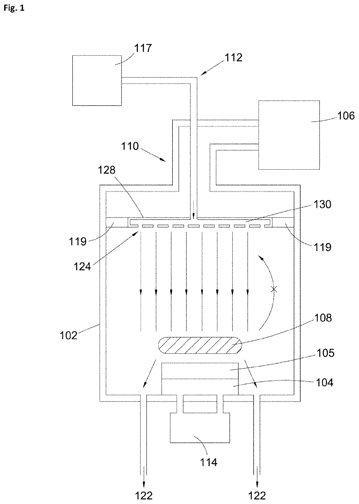
[0048]As previously described in the summary of invention section, a method of fabricating synthetic diamond material using a microwave plasma activated chemical vapour deposition technique is provided which utilizes high and uniform microwave power densities applied over large areas and for extended periods of time.

[0049]The microwave power density may be maintained at a power density of at least 3.2 W / mm2, 3.4 W / mm2, or 3.6 W / mm2 and / or no more than 10 W / mm2, 8 W / mm2, 6 W / mm2, 5 W / mm2, or 4 W / mm2. The optimal power density within these ranges will be dependent on the precise product which is being fabricated.

[0050]Furthermore, the microwave power density is maintained at a target value with a variation over time of no more than ±5%, ±3%, ±2%, or ±1% as measured by fluctuations in total microwave power input to the plasma chamber averaged over 5 second measurement periods for a time period forming at least 30%, 50%, 70%, 90%, or 95% of a total growth time period. For example, the m...


PUM

PropertyMeasurementUnit
areaaaaaaaaaaa
surface areaaaaaaaaaaa

Abstract

A method of fabricating synthetic diamond material using a microwave plasma activated chemical vapour deposition technique is provided which utilizes high and uniform microwave power densities applied over large areas and for extended periods of time. Products fabricated using such a synthesis technique are described including a single crystal CVD diamond layer which has a large area and a low nitrogen concentration, and a high purity, fast growth rate single crystal CVD diamond material.

Description

CROSS REFERENCE TO RELATED APPLICATIONS[0001]This application is a divisional application of U.S. patent application Ser. No. 15 / 036,692 filed on May 13, 2016 which is a U.S. national phase of International Application No. PCT / EP2014 / 074864 filed on Nov. 18, 2014, and published in English on May 21, 2015 as International Publication No. WO 2015 / 071484 A1, which application claims priority to Great Britain Patent Application No. 1320304.7 filed on Nov. 18, 2013, the contents of which are incorporated herein by reference.FIELD OF INVENTION[0002]The present invention relates to methods of fabricating synthetic diamond materials using microwave plasma active chemical vapour deposition techniques and products obtained using said methods. Products comprising very high purity single crystal synthetic diamond material are described and method of manufacturing the same at increased growth rates while retaining exceptional electronic, optical, thermal, and / or quantum coherence characteristics...

Claims


Application Information

Patent Timeline
Patent Type & Authority Applications(United States)
IPC IPC(8): C30B25/10C23C16/27C30B29/04C23C16/511
CPCC30B25/105C23C16/511C30B29/04C23C16/274C23C16/52C01B32/25
Inventor KHAN, RIZWANCOE, STEVENWILMAN (DECEASED), JONATHANTWITCHEN, DANIELSCARSBROOK, GEOFFREYBRANDON, JOHNWORT, CHRISTOPHERMARKHAM, MATTHEWFRIEL, IANROBERTSON, KATHARINE
Owner ELEMENT SIX TECH LTD
Why Eureka
Try Eureka