Semiconductor device and charge control system

a technology of magnetic field and control system, which is applied in the direction of secondary battery servicing/maintenance, safety/protection circuit, electrochemical generator, etc., can solve the problems of overcharging, adverse influence, and thermal runaway of secondary battery using lithium ions, so as to reduce damage to the battery and quickly stop charging, the effect of reducing the function

Pending Publication Date: 2022-02-10
SEMICON ENERGY LAB CO LTD
View PDF2 Cites 2 Cited by
  • Summary
  • Abstract
  • Description
  • Claims
  • Application Information

AI Technical Summary

Benefits of technology

[0054]Blocking two paths which connect to a battery can quickly stop charging when overcharge is detected and reduce damage to the battery owing to the overcharge.
[0055]When one flexible sheet provided on a side surface of a battery is provided with a protection circuit, a charge control circuit, and an abnormality detection circuit, a printed board on which these circuits are mounted as a plurality of IC chips is not needed, achieving a miniaturized electronic device without reducing the functions.

Problems solved by technology

Moreover, a secondary battery using lithium ions is known to exhibit thermal runaway with an internal short circuit, overcharge, or the like due to degradation.
However, if abnormality is caused in at least one of the batteries, the other secondary batteries are adversely influenced and a protection circuit may operate to stop the use of the assembled battery.
The smallness of the housing of the portable information terminal and large capacity of secondary batteries are desired; however, there is a space limitation in the housing.

Method used


Image

  • Semiconductor device and charge control system
  • Semiconductor device and charge control system
  • Semiconductor device and charge control system

Examples


embodiment 1

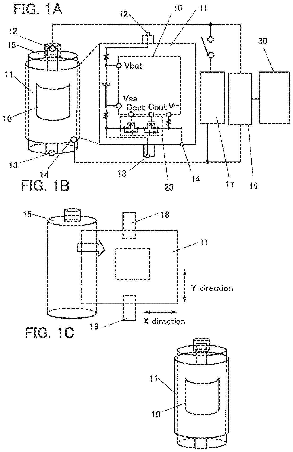
[0076]FIG. 1A is a conceptual diagram of a charge control system for wireless charging, where a charge control circuit 10 formed over a flexible substrate 11, which is a flexible film, is mounted on a cylindrical secondary battery 15. Note that in FIG. 1A, Vbat is a voltage of the secondary battery, Vss and V− are voltages of the charge control circuit, and Dout and Cout are output terminals. The charge control system includes at least the cylindrical secondary battery 15, the charge control circuit 10, a first switch 20, a charging circuit 16, and an antenna 30.

[0077]The cylindrical secondary battery 15 includes a first terminal 12 on the top surface and a second terminal 13 on the bottom surface. A first transmission path which is connected to the first terminal 12 of the cylindrical secondary battery and through which electric power output from the cylindrical secondary battery 15 is transmitted is electrically connected to a terminal of the charge control circuit through an elec...

embodiment 2

[0125]In this embodiment, another structure example of the cylindrical secondary battery of Embodiment 1 will be described with reference to FIG. 5 and FIG. 6.

[0126]FIG. 5A is a diagram illustrating an external view of a battery pack which includes a secondary battery 913 having a flat shape, a charge control circuit 914, and a connection terminal 911.

[0127]The charge control circuit 914 is formed over or fixed to a flexible substrate 910. The charge control circuit 914 detects abnormality such as a micro-short circuit. Furthermore, the charge control circuit 914 may have a function of a protection circuit for protecting the secondary battery 913 from overcharge, overdischarge, and an overcurrent.

[0128]As the charge control circuit 914, the charge control circuit 10 described in Embodiment 1 can be used. Since the same circuit structure and the like can be used, the detailed description thereof is omitted here.

[0129]In addition to the charge control circuit 914, the antenna and the ...

embodiment 3

[0141]In this embodiment, a structure example of an OS transistor that can be used in the charge control circuit 10 described in the above embodiment will be described. Note that the OS transistor is a thin film transistor and can be formed over a separation layer provided over a glass substrate or stacked over a single crystal silicon substrate.

[0142]Embodiment 1 shows an example in which a flexible substrate provided with a charge control circuit is bonded to a curved surface of a secondary battery, where an OS transistor formed over a separation layer provided over a glass substrate is fixed to the flexible substrate by a known separation method. Furthermore, Embodiment 2 shows an example in which a charge control circuit is bonded to a flat surface of a secondary battery, where after an OS transistor is formed over a single crystal silicon substrate, a rear surface of the single crystal silicon substrate is polished and the thinned single crystal silicon substrate is fixed to a ...


PUM

PropertyMeasurementUnit
temperaturesaaaaaaaaaa
lengthaaaaaaaaaa
lengthaaaaaaaaaa

Abstract

A structure that includes a circuit for controlling the safe operation of a secondary battery but can overcome space limitations owing to miniaturization of the housing is provided. A charge control circuit is provided over a flexible substrate and bonded to an external surface of the secondary battery. The charge control circuit is electrically connected to at least one of two terminals of the secondary battery and controls charging. To prevent overcharge, both an output transistor of a charging circuit and a blocking switch are brought into off state substantially concurrently. Blocking two paths which connect to the battery can quickly stop charging when overcharge is detected and reduce damage to the battery owing to the overcharge.

Description

TECHNICAL FIELD[0001]One embodiment of the present invention relates to an object, a method, or a manufacturing method. Alternatively, the present invention relates to a process, a machine, manufacture, or a composition (composition of matter). One embodiment of the present invention relates to a semiconductor device, a display device, a light-emitting device, a power storage device, a lighting device, an electronic device, or a manufacturing method thereof. In particular, the present invention relates to a semiconductor device using an oxide semiconductor and a manufacturing method thereof.[0002]Note that in this specification, a semiconductor device refers to any device that can function by utilizing semiconductor characteristics, and an electro-optical device, a semiconductor circuit, and an electronic device are all semiconductor devices.[0003]Furthermore, one embodiment of the present invention relates to a charge control system using an oxide semiconductor, a charge control me...

Claims


Application Information

Patent Timeline
Patent Type & Authority Applications(United States)
IPC IPC(8): H02J7/00H02J50/10H01M10/44
CPCH02J7/00302H01L23/5223H01M10/44H02J50/10H01M10/48H02H7/18Y02E60/10H01L29/78696H01L29/7869H01L29/78648H02J7/0031H02J7/06H01L29/7851
Inventor ONUKI, TATSUYAIKEDA, TAKAYUKIYAMAZAKI, SHUNPEI
Owner SEMICON ENERGY LAB CO LTD
Why Eureka
Try Eureka