Electrostatic discharge protection device and operating method

Pending Publication Date: 2022-07-21
MACRONIX INT CO LTD
View PDF4 Cites 0 Cited by
  • Summary
  • Abstract
  • Description
  • Claims
  • Application Information

AI Technical Summary

Benefits of technology

[0005]The present invention relates to an electrostatic discharge protection device and an operating method thereof, which can solve the problem that the conventi

Problems solved by technology

Semiconductor integrated circuit (IC) is vulnerable to ESD events resulted by human or machines contact with the leads of the IC, and thus ESD currents pass t

Method used


Image

  • Electrostatic discharge protection device and operating method
  • Electrostatic discharge protection device and operating method
  • Electrostatic discharge protection device and operating method

Examples


Example

First Embodiment

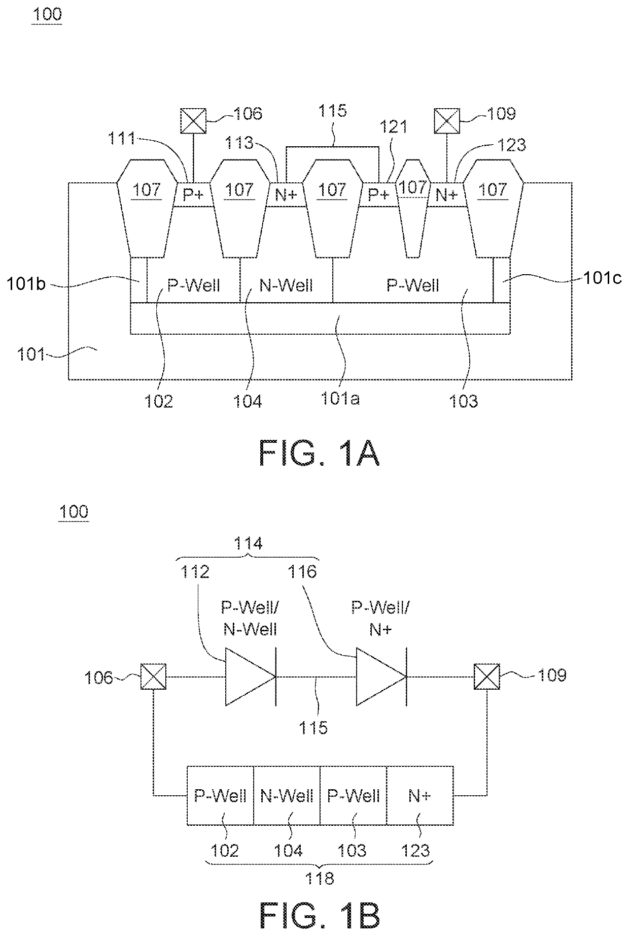
[0018]Please refer to FIGS. 1A and 1B, which respectively show a cross-sectional schematic diagram of an ESD device 100 and a schematic diagram of its equivalent circuit according to an embodiment of the invention.

[0019]According to an embodiment of the invention, the ESD device 100 includes a semiconductor substrate 101, a first well 102, a second well 103, a third well 104, a first doping region 111, a second doping region 113, a third doping region 121, and a fourth doping region 123.

[0020]In an embodiment, the semiconductor substrate 101 can be made of a suitable basic semiconductor (such as silicon (Si) or germanium (Ge) and so on), a compound semiconductor (such as silicon carbide (SiC), gallium arsenide (GaAs), gallium phosphide (GaP), iodine phosphide (IP), iodine arsenic (IAs) and / or iodine antimony (ISb)) or a combination thereof. The semiconductor substrate 101 is, for example, a P-type substrate. The semiconductor substrate 101 includes a first well 102 a...

Example

Second Embodiment

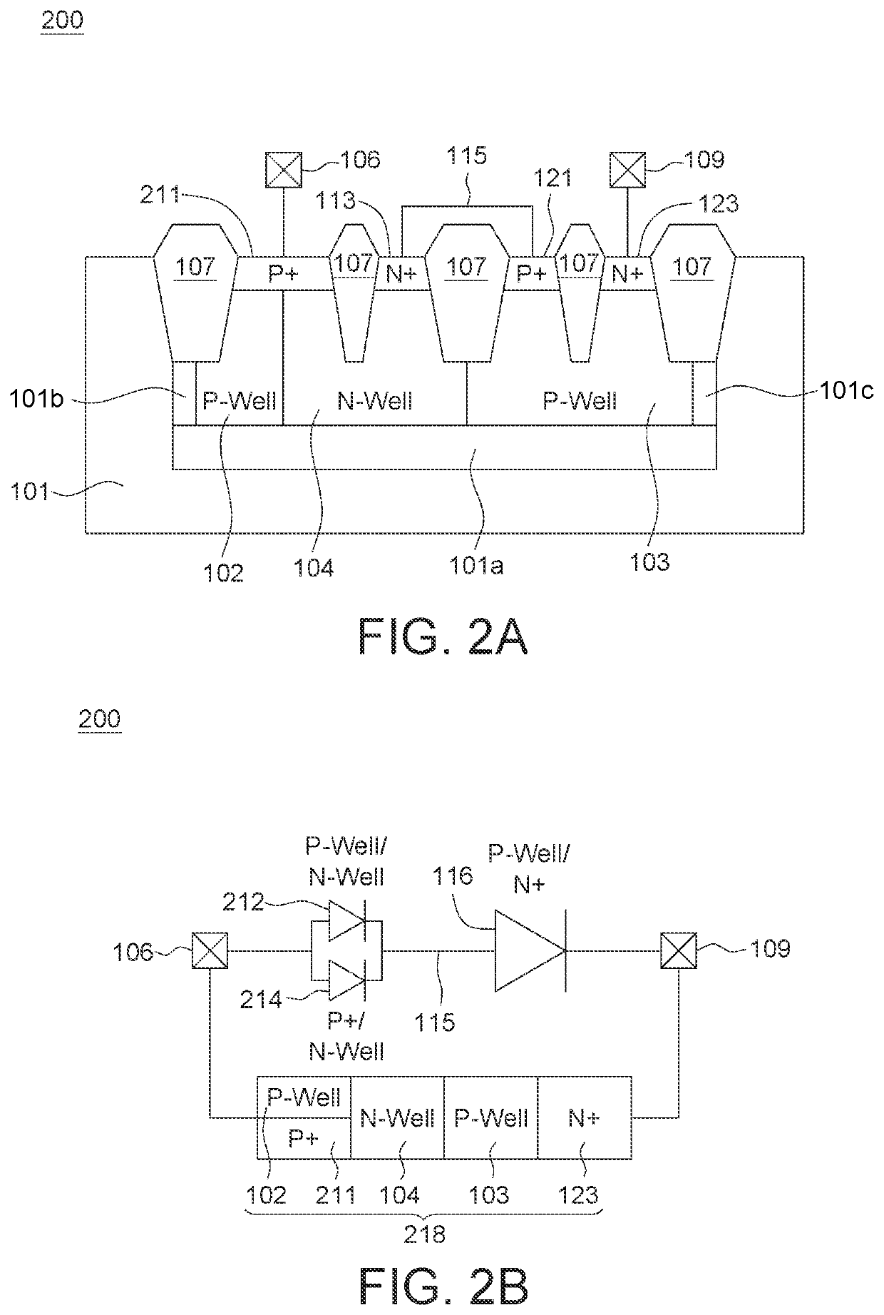
[0028]Please refer to FIGS. 2A and 2B, which respectively show a cross-sectional schematic diagram of an ESD device 200 and a schematic diagram of its equivalent circuit according to another embodiment of the invention. The structure of the ESD device 200 is analog to the structure of the ESD device 100 shown in FIG. 1A, except that a part of the first doping region 211 is disposed in the first well 102, and another part of the first doping region 211 is disposed in the third well 104. The first doping region 211 is analog to the first doping region 111.

[0029]In the ESD device 200, there are two diodes connected in parallel, in which the first well 102 and the third well 104 are coupled to form a diode 212, and the first doping region 211 and the third well 104 are coupled to form another diode 214, thereby the effective circuit path of ESD is increased.

[0030]In addition, when ESD stress is applied to the internal circuit protected by the ESD device 200, the ESD cur...

Example

Third Embodiment

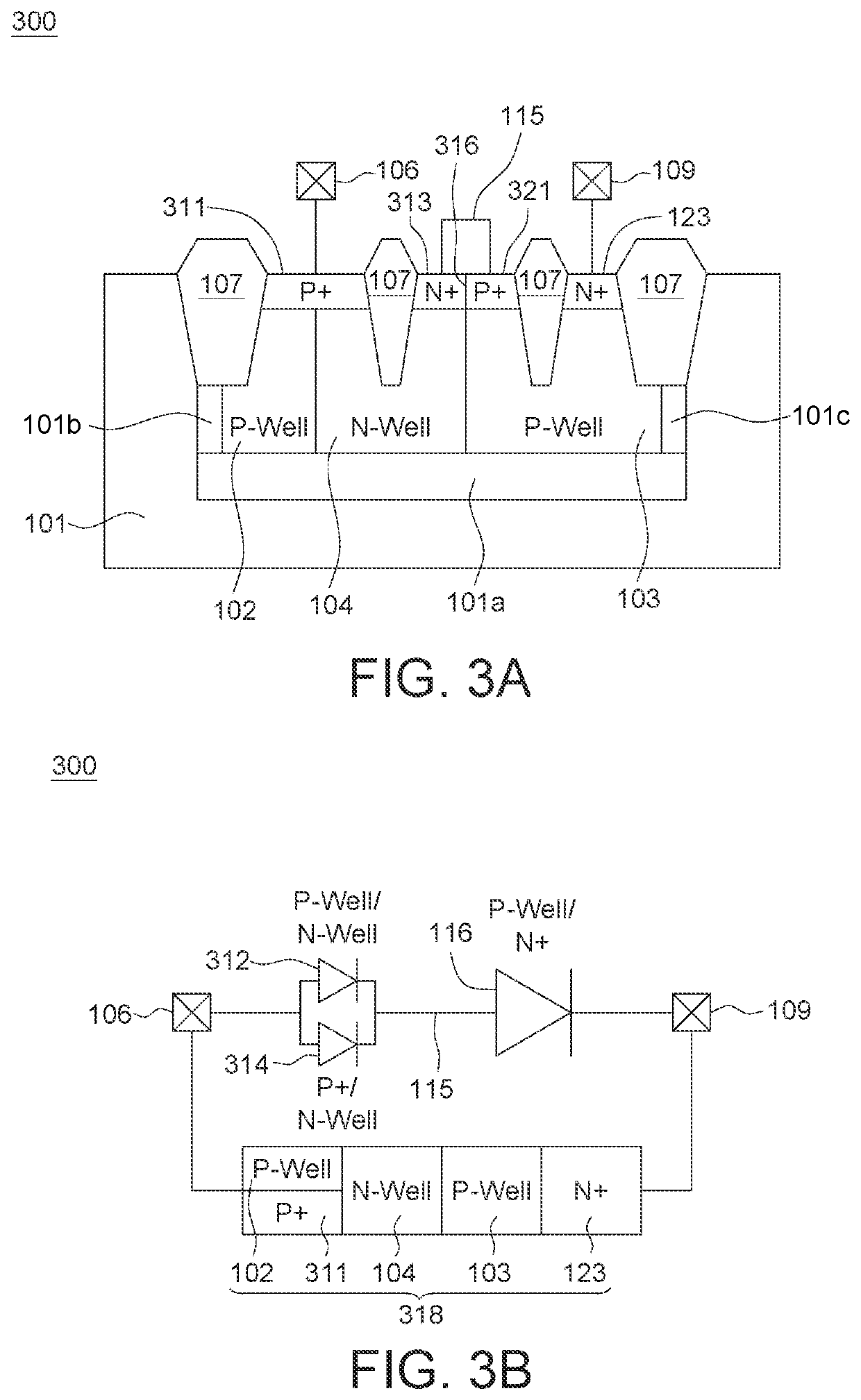
[0033]Please refer to FIGS. 3A and 3B, which respectively show a cross-sectional schematic diagram of an ESD device and a schematic diagram of its equivalent circuit according to another embodiment of the present invention. The structure of the ESD device 300 is analog to that of the ESD device 100 shown in FIG. 1A, except that a part of the first doping region 311 is disposed in the first well 102, another part of the first doping region 311 is disposed in the third well 104, and the second doping region 313 and the third doping region 321 are directly connected to each other to form a junction 316. The first doping region 311, the second doping region 313 and the third doping region 321 are analog to the first doping region 111, the second doping region 113 and the third doping region 121.

[0034]In the ESD device 300, there are two diodes connected in parallel, in which the first well 102 and the second well 103 are connected to form a diode 312, and the first dopin...


PUM


Abstract

An ESD protection device includes a semiconductor substrate, a first well, a second well, a third well, a first doping region, a second doping region, a second doping region, a third doping region and a fourth doping region. The first well and the second well have a first conductivity, and the third well has a second conductivity. The first doping region having a first conductivity is disposed in the first well. The second doping region having a second conductivity is disposed in the third well, and the first and the second doping regions are isolated from each other. The third doping region and the fourth doping region have a first conductivity and a second conductivity, respectively. The second doping region and the third doping region are electrically coupled. The first well, the second well, the third well and the fourth doping region form a parasitic SCR.

Description

BACKGROUND OF THE INVENTIONField of the Invention[0001]The invention relates in general to a semiconductor device, and more particularly to an electrostatic discharge (ESD) protection device and an operating method thereof.Description of the Related Art[0002]An ESD event commonly results from the discharge of a high voltage potential and leads to pulses of high current in a short duration (typically, 100 nanoseconds). Semiconductor integrated circuit (IC) is vulnerable to ESD events resulted by human or machines contact with the leads of the IC, and thus ESD currents pass through the IC to make the component failure. Accordingly, an ESD protection circuit is essential to a semiconductor IC.[0003]A parasitic silicon controlled rectifier (SCR) is one kind of on-chip semiconductor ESD protection device. SCR can be turned on by snapback when ESD zapping occurs, and conduct ESD current to the ground to achieve ESD protection, so that parasitic SCR have been recognized in the prior art as...

Claims


Application Information

Patent Timeline
IPC IPC(8): H01L27/02H01L29/74
CPCH01L27/0248H01L29/7436H01L27/0262H01L27/0296H01L29/861H01L29/87H01L29/0649H01L27/0255
Inventor WANG, SHIH-YUHSU, CHIH-WEIHUANG, WEN-TSUNG
Owner MACRONIX INT CO LTD
Why Eureka
Try Eureka