Semiconductor treatment liquid

a technology of semiconductor elements and treatment liquid, applied in the direction of semiconductor/solid-state device manufacturing, basic electric elements, electric devices, etc., can solve the problems of etching, needing countermeasures, and marked impairment of high-speed operations of semiconductor elements, so as to reduce the roughness of the transition metal surface after etching, the effect of sufficient rate and stable

Pending Publication Date: 2022-10-13
TOKUYAMA CORP
View PDF0 Cites 0 Cited by
  • Summary
  • Abstract
  • Description
  • Claims
  • Application Information

AI Technical Summary

Benefits of technology

[0053]According to the semiconductor treatment liquid of the present invention, a transition metal can be stably wet-etched at a sufficient rate in a semiconductor formation process. In addition, the roughness of the transition metal surface after etching can be reduced, and the flatness can be maintained. By all of these effects, not only the accuracy of processing a transition metal contained in a semiconductor wafer and the yield are improved, but also the wa

Problems solved by technology

As a result of the increase in the wiring resistance, the high-speed operations of semiconductor elements have been markedly impaired, making it necessary to take countermeasures.
However, for ruthenium, tungsten, molybdenum, and chromium, since etching in a dry state using an etching gas and etching/removal by CMP polishing are difficult, a mor

Method used


Image

  • Semiconductor treatment liquid
  • Semiconductor treatment liquid
  • Semiconductor treatment liquid

Examples


example 1

(Method of Producing Treatment Liquid Containing Tetramethylammonium Hypobromite)

(Step of Preparing Solution Containing Bromine Salt and Organic Alkali)

[0222]Tetramethylammonium bromide (14.6 g; 0.095 mol) and tetramethylammonium hydroxide (18.2 g; 0.190 mol) were put into a 2-L three-necked glass flask (manufactured by Cosmos Bead Co., Ltd.), and ultrapure water was added thereto to prepare 1 L of a solution which had a pH of 13.3 and contained a bromine salt and an organic alkali.

(Step of Allowing Solution Containing Bromine Salt and Organic Alkali to React with Halogen)

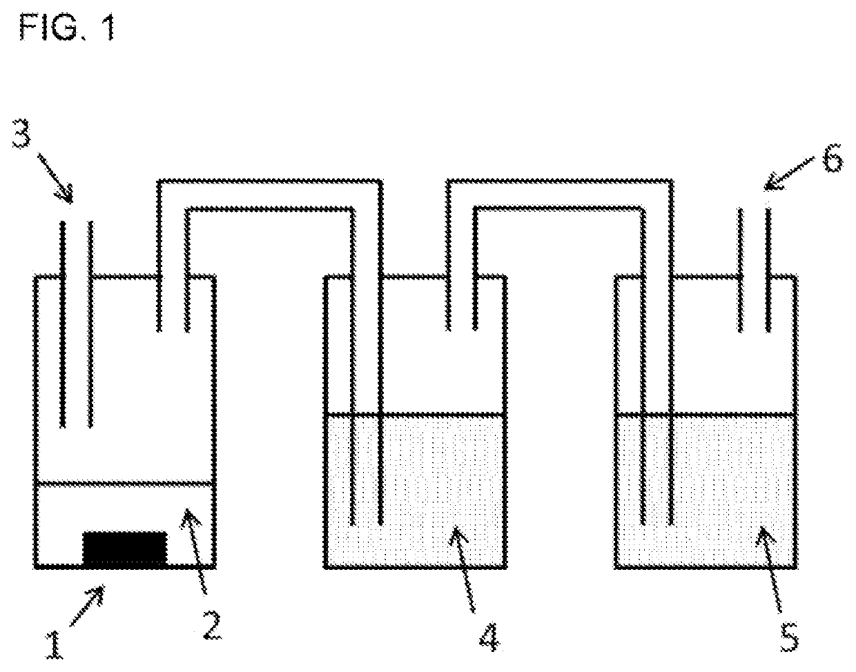
[0223]Subsequently, a stirrer bar (30 mm in total length×8 mm in diameter, manufactured by As One Corporation) was put into the three-necked flask, and a thermometer protection tube (bottom-closed type, manufactured by Cosmos Bead Co., Ltd.) and a thermometer were inserted through one of the openings. Through other opening, a tip of a PFA tube (F8011-02, manufactured by Flon Industry Co., Ltd.), which was connected...

examples 2 to 12

[0226]Halogen oxyacid-containing treatment liquids shown in Table 1 were obtained in the same manner as in “Method of Producing Treatment Liquid Containing Tetramethylammonium Hypobromite” described in Example 1, except that the concentrations of the bromine salt and the organic alkali and the supply amount of chlorine gas were adjusted as appropriate. The thus obtained treatment liquids were evaluated in the same manner as in Example 1. The results thereof are shown in Tables 2 and 3.

examples 13 to 16

[0227]Halogen oxyacids were obtained in the same manner as in “Method of Producing Treatment Liquid Containing Tetramethylammonium Hypobromite” described in Example 1, except that the concentrations of the bromine salt and the organic alkali and the supply amount of chlorine gas were adjusted as appropriate. It is noted here that, in Example 15, the flask was heated and chlorine gas was supplied at a solution temperature of 45° C. for generation of bromite ions. The thus obtained halogen oxyacids were each diluted to 1 / 100 by mixing with tetramethylammonium bromate, ultrapure water, 15%-by-weight HCl, and 1-mol / L TMAH, whereby treatment liquids having the respective formulations shown in Table 1 were obtained each in an amount of 100 mL. The thus obtained treatment liquids were evaluated in the same manner as in Example 1. The results thereof are shown in Tables 2 and 3.


PUM


Abstract

Provided are: a semiconductor treatment liquid containing a hypobromite ion, in which the concentration of the hypobromite ion is 0.1 μmol/L or more and less than 0.001 mol/L; a RuO4 gas generation inhibitor containing an onium salt composed of an onium ion and a bromine-containing ion, in which the hypobromite ion concentration is 0.1 μmol/L or more and less than 0.001 mol/L; and a method of producing a halogen oxyacid, the method including allowing a bromine salt, an organic alkali, and a halogen to react with each other to obtain the halogen oxyacid.

Description

BACKGROUND OF THE INVENTIONField of the Invention[0001]The present invention relates to a semiconductor treatment liquid containing a hypobromite ion (hereinafter, also simply referred to as “treatment liquid”), in which the concentration of the hypobromite ion is 0.1 μmol / L or more and less than 0.001 mol / L. The present invention also relates to a RuO4 gas generation inhibitor containing an onium salt composed of an onium ion and a bromine-containing ion, in which the concentration of a hypobromite ion is 0.1 μmol / L or more and less than 0.001 mol / L. Further, the present invention relates to a method of producing a halogen oxyacid.BACKGROUND ART[0002]In recent years, the design rules for semiconductor elements have been refined, and the wiring resistance tends to be increased. As a result of the increase in the wiring resistance, the high-speed operations of semiconductor elements have been markedly impaired, making it necessary to take countermeasures. In light of this, a wiring m...

Claims


Application Information

Patent Timeline
IPC IPC(8): H01L21/306
CPCH01L21/30604H01L21/32134C23F1/40C23F1/14C23F1/10C23F1/46
Inventor KIKKAWA, YUKISATO, TOMOAKINEGISHI, TAKAYUKI
Owner TOKUYAMA CORP
Why Eureka
Try Eureka