Electronic circuit component

a technology of electronic circuit and components, applied in the direction of superconductor devices, instruments, transportation and packaging, etc., can solve the problems of low adhesion strength between the insulating film and the insulating film, and the inability to perform the high-speed operation of the superconducting josephson device,

Inactive Publication Date: 2000-05-09
KYOCERA CORP
View PDF6 Cites 11 Cited by
  • Summary
  • Abstract
  • Description
  • Claims
  • Application Information

AI Technical Summary

Problems solved by technology

However, as an operation speed of the superconducting Josephson device has increased recently, the dielectric constant of 3 to 3.5 and a dielectric loss of about 20.times.10.sup.-5 of the conventional polyimide resin have become so great that it is difficult to accomplish a high-speed transmission of signals and, in turn, it is impossible to perform the high-speed operation in the superconducting Josephson device.
However, the following problem exists in the multi-layered circuit substrate using the insulating film made of a high polymer material such as the fluorine-containing polymer or the fluorine-containing cycloaliphatic polymer and using the circuit conductive layer made of the superconducting metal.
That is, an adhesion strength is low between the insulating film made of the fluorine-containing polymer or the fluorine-containing cycloaliphatic polymer and the circuit conductive layer made of the superconducting metal, because functional groups composi...

Method used


Image

  • Electronic circuit component

Examples


Embodiment Construction

Now, an effect of the invention will be described with reference to an example hereof.

(Preparation of Evaluation Samples)

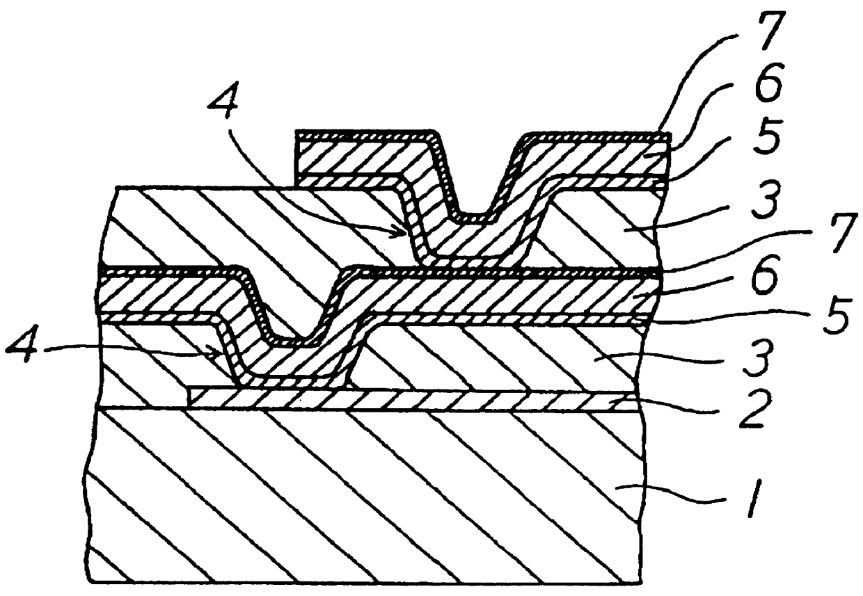
On a surface of an insulating substrate made of alumina ceramics having a thickness of 0.635 mm and dimensions of 50-mm square, a film of aluminum was formed so as to have a thickness of 1 .mu.m by sputtering, and a lower conductive layer pattern was formed by means of the photolithography technique.

Subsequently, a cyclized polyethylene fluoride resin was applied by spin coating onto each surface of the insulating substrate and lower conductive layer pattern, and was heat-treated at 300.degree. C. to form a 3-.mu.m-thick insulating film.

Subsequently, on this insulating film, a film of copper having a thickness shown in Table 1, a film of niobium having a thickness of 1 to 3 .mu.m and further a film of copper having a thickness of 2 to 3 .mu.m were sequentially formed by means of sputtering, respectively serving as a base metal layer, a circuit conductive layer and...


PUM

PropertyMeasurementUnit
Water absorptionaaaaaaaaaa
Lengthaaaaaaaaaa
Lengthaaaaaaaaaa

Abstract

A prior-art electronic circuit component comprising an insulating film and a circuit conductive layer made of a superconducting metal suffers low reliability resulting from insufficient adhesion between these layers. An electronic circuit component of the invention comprises an insulating film made of a high polymer material having a dielectric constant of 2.5 or less, a base metal layer formed of copper on the insulating film, having a thickness of 0.01 to 0.3 mu m, and a circuit conductive layer formed of at least one of niobium and niobium nitride on the base metal layer. The electronic circuit component of the invention can accomplish an increased adhesion between the insulating film and the circuit conductive layer. Furthermore, by sequentially forming, on the circuit conductive layer, a conductive-layer coating metal layer made of at least one of aluminum and copper, the insulating film, the base metal layer and the circuit conductive layer, there can be obtained a multi-layered circuit substrate with a superconducting circuit of high density and high-level function.

Description

1. Field of the InventionThe present invention relates to an electronic circuit component and more particularly to an improvement in adhesion between a circuit conductive layer and an insulating film disposed in such an electronic circuit component as a multi-layered circuit substrate, including the insulating film made of a high polymer material between layers and the circuit conductive layer made of a superconducting metal.2. Description of the Related ArtConventionally, a circuit conductive layer of an electronic circuit component such as a multi-layered circuit substrate on which a Josephson device made of a superconducting material is mounted, is essentially fabricated by the steps of: forming an insulating film made of a polyimide resin with a relatively small dielectric constant of 3 to 3.5 on a substrate made of such a material having an excellent insluating property as alumina, mullite, silicon or the like; forming thereover a circuit conductive layer made of niobium (Nb), ...

Claims


Application Information

Patent Timeline
IPC IPC(8): H01L23/52H01L23/532H01L21/312H01L21/3205H05K1/09H01L27/01H01L39/00H05K1/03
CPCH01L23/53285H01L2924/0002Y10T428/263H01L2924/00Y10T428/31678
Inventor TANAHASHI, SHIGEOYAMAJI, TOKUICHI
Owner KYOCERA CORP
Why Eureka
Try Eureka