

Method of forming films over insulating material
a technology of insulating material and film, which is applied in the field of forming films over insulating materials, can solve the problems of affecting prone to attract contaminants and dust in the atmosphere, so as to reduce prevent the generation of dust caused by abrasion, and improve the surface electrical resistance value
- Summary
- Abstract
- Description
- Claims
- Application Information
AI Technical Summary
Benefits of technology
Problems solved by technology
Method used
Image

Examples
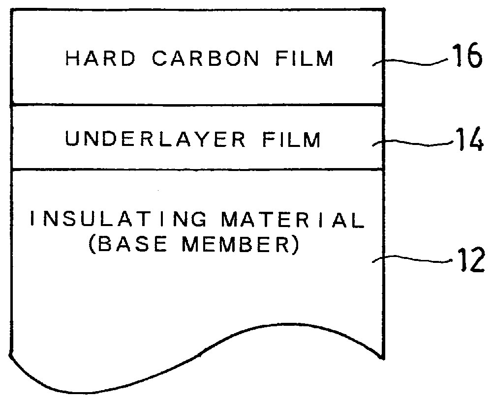
first embodiment
FIG. 1 is a schematic sectional view illustrating the construction of films formed over an insulating material by a first embodiment of a method according to the invention.
In the construction shown in FIG. 1, a hard carbon film 16 is provided via an underlayer film 14 formed over an insulating material 12 comprising a base member of various components, jigs, tools, or the like. The insulating material 12 is glass, ceramic, resin (plastics), or the like.
A metal film or semiconductor film as the underlayer film 14 is formed on the surface of the insulating material 12. The underlayer film 14 is formed by means of a physical vapor deposition method, such as the sputtering method, vacuum deposition method or the like, or the CVD (chemical vapor deposition) method.
Then, the hard carbon film 16 is formed over the underlayer film 14. The hard carbon film 16 is formed by means of the plasma CVD method using methane (CH.sub.4) as feed gas.
In the case of a metal film being used for the underl...
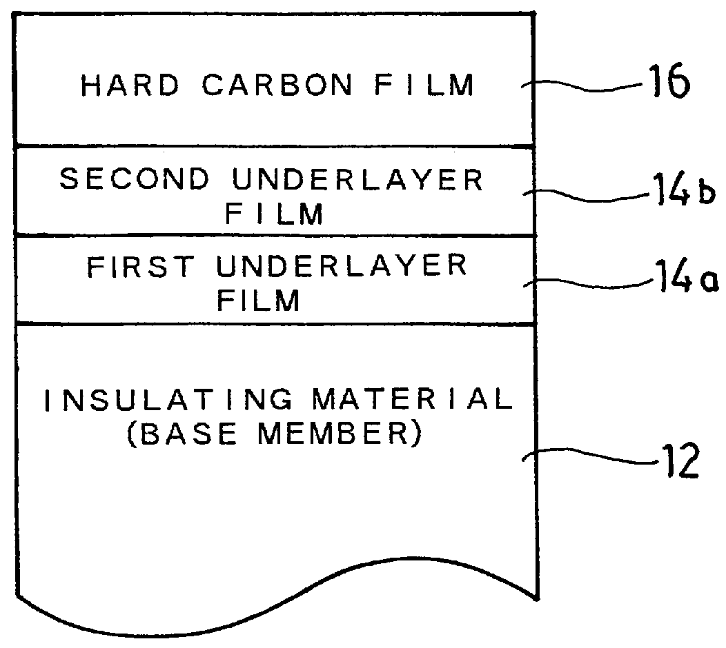
second embodiment
Next, a second embodiment according to the invention will be described hereinafter. FIG. 3 is a schematic sectional view illustrating the construction of the films formed over an insulating material.
In the construction shown in FIG. 3, a hard carbon film 16 is provided via a first underlayer film 14a and second underlayer film 14b formed over an insulating material 12 comprising a base member of various components, jigs, tools, or the like. The insulating material 12 is glass, ceramic, resin (plastics), or the like.
For the first underlayer film 14a, a metal film composed of a metal selected from the group consisting of titanium (Ti), chromium (Cr), tungsten (W), or a compound such as a carbide, nitride, or the like of one of the aforesaid metals is formed on the surface of the insulating material 12.
For the second underlayer film 14b, a semiconductor film composed of silicon (Si), germanium (Ge), or the like is formed over the first underlayer film 14a.
The underlayer films 14a, 14b ...
third embodiment
Next, the third embodiment according to the invention will be described hereinafter. FIG. 5 is a schematic sectional view illustrating the construction of the films formed over an insulating material.
In the construction shown in FIG. 5, a hard carbon film 16 is provided via a first underlayer film 14a, second underlayer film 14c, and third underlayer film 14d, formed over an insulating material 12 comprising a base member of various components, jigs, tools, or the like. The insulating material 12 is glass, ceramic, resin (plastics), or the like.
For the first underlayer film 14a, a metal film composed of a metal selected from the group consisting of titanium (Ti), chromium (Cr), tungsten (W), or a compound such as a carbide, nitride, or the like, of one of the aforesaid metals is formed to a thickness in the range of 0.1 to 0.2 .mu.m on the surface of the insulating material 12.
For the second underlayer film 14c, a metal film composed of a metal selected from the group consisting of ...
PUM
| Property | Measurement | Unit |
|---|---|---|
| electrical resistance | aaaaa | aaaaa |
| surface electrical resistance | aaaaa | aaaaa |
| thick | aaaaa | aaaaa |
Abstract
Description
Claims
Application Information