Leadless ceramic chip carrier crosstalk suppression method

a ceramic chip and chip carrier technology, applied in piezoelectric/electrostrictive transducers, electrical apparatus construction details, manufacturing tools, etc., can solve problems such as troublesome sources of interference, particularly acute thermal mismatch problems, and large distance between soldering pads, so as to reduce electromagnetic signal effects or crosstalk, enhance crosstalk suppression, and enhance crosstalk suppression

Inactive Publication Date: 2000-08-22
TRIQUINT
View PDF16 Cites 41 Cited by
  • Summary
  • Abstract
  • Description
  • Claims
  • Application Information

AI Technical Summary

Benefits of technology

It is a primary object of the invention to reduce electromagnetic signal effects or crosstalk between SAW device input and output connections. It is another object of the invention to provide improved grounding within a surface mount package for enhancing crosstalk suppression. It is an object to enhance crosstalk suppression while maintaining package size for optimum efficiency in circuit design and reduction of thermal mismatch effects. It is another object of the present invention to provide sufficient grounding of a surface mount package for enhancing the desired response of a SAW device carried by the package. It is yet another object of the invention to provide improved grounding between the seal ring of a surface mount package and common ground pads. It is further an object of the invention to provide sufficient separation between input and output bond connections within the surface mount package for reducing crosstalk while maintaining a bond pad configuration for connection to PC board pads that minimizes thermal expansion concerns.

Problems solved by technology

In particular, the thermal mismatch problems are especially acute for relatively large leadless chip carrier in which the distance between soldering pads is also relatively large.
In addition to the thermal mismatch problems, electromagnetic feedthrough, also referred to as crosstalk, between input and output circuits create undesired effects and can be one of the most troublesome sources of interference in SAW devices.
By way of example, if in a design of a SAW filter, crosstalk is not sufficiently suppressed, the desired frequency response of the filter will not be achieved.
Further, in leadless chip ceramic carriers (LCCC) typical in the art, grounding between the seal ring at the upper end of a package and the customer common pads on the package bottom side does not provide a sufficient ground path to adequately suppress crosstalk and thus SAW device performance is adversely affected.
In some cases, crosstalk is actually enhanced by an inadequate ground path.
This series and parallel combination styled grounding path does not provide sufficient RF grounding for the SAW devices earlier described.

Method used


Image

  • Leadless ceramic chip carrier crosstalk suppression method
  • Leadless ceramic chip carrier crosstalk suppression method
  • Leadless ceramic chip carrier crosstalk suppression method

Examples


Embodiment Construction

The present invention will now be described more fully hereinafter with reference to the accompanying drawings, in which preferred embodiments of the invention are shown. This invention may, however, be embodied in many different forms and should not be construed as limited to the embodiments set forth herein. Rather, these embodiments are provided so that this disclosure will be thorough and complete, and will fully convey the scope of the invention to those skilled in the art. Like numbers refer to like elements throughout.

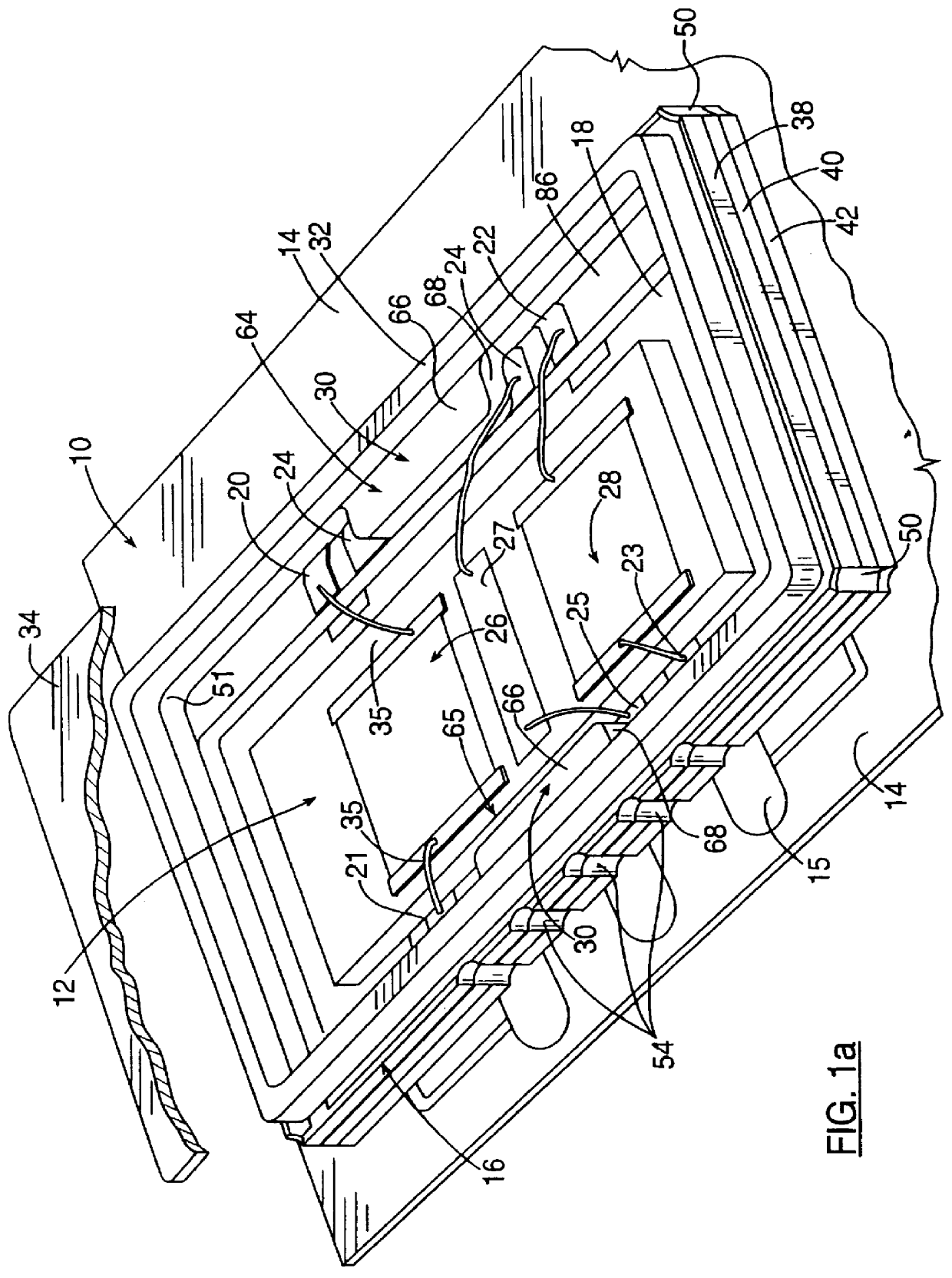
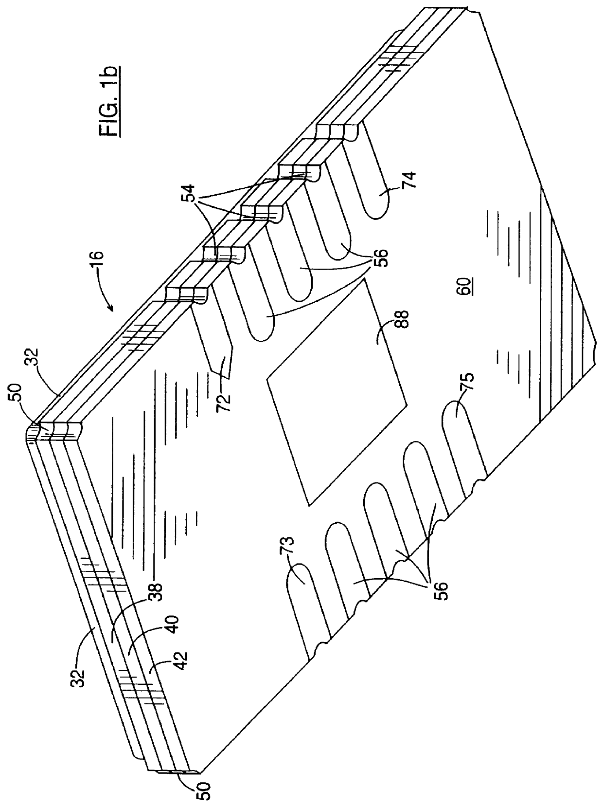
Referring now to FIGS. 1a and 1b, a preferred embodiment of the present invention, a surface mount package 10 for mounting a SAW device 12 onto a printer circuit board 14. The package 10 comprises a leadless ceramic chip carrier 16 having a cavity portion 18 for receiving the device 12. Within the carrier cavity portion 18, input bond pads 20, 21, wire bonded to device input transducer 26, output bond pads 22, 23 wire bonded to output transducer 28, and ground b...


PUM

PropertyMeasurementUnit
electricallyaaaaaaaaaa
conductiveaaaaaaaaaa
electricalaaaaaaaaaa

Abstract

A leadless ceramic chip carrier useful in surface mounting of SAW devices includes electrically conductive vias and metalization between input and output bond pads for improved crosstalk suppression between input and output device connections. A protrusion extending from a top layer of a multilayer ceramic carrier provides additional electrical contact to a package seal brazed thereto. The vias are positioned between input and output bond pads and connect the metalized protrusion to package ground pads through contact with multiple metalized layers of the package for enhancing the electrical connection between the package Kovar seal ring and customer accessed ground pads. For further suppression of crosstalk, bond pads within the package for connection to the SAW device are spaced at a greater distance from each other than their corresponding pads on the package bottom surface thus maintaining an optimum spacing for package connection to printed circuit board pads for minimizing thermal mismatch effects.

Description

BACKGROUND OF INVENTION1. Field of InventionThe invention relates to printed circuit board surface mounted electronic chip packaging and more particularly to decreasing crosstalk or electromagnetic feedthrough in leadless ceramic chip carriers for surface acoustic wave filters.2. Description of Background ArtSurface mount technology offers several advantages for electronic equipment manufacturers including the economic advantage of increased component packing density. As described in U.S. Pat. No. 5,369,551 to Gore et al., surface mount technology carries with it the problem of thermal mismatch between the surface mount package and the printed circuit (PC) board. In particular, the thermal mismatch problems are especially acute for relatively large leadless chip carrier in which the distance between soldering pads is also relatively large.In addition to the thermal mismatch problems, electromagnetic feedthrough, also referred to as crosstalk, between input and output circuits create...

Claims


Application Information

Patent Timeline
Patent Type & Authority Patents(United States)
IPC IPC(8): H01L23/66H01L23/58H01L23/498H01L23/48H03H9/10H03H9/05H03H9/00
CPCH01L23/49805H03H9/1071H01L23/66Y10T29/42H01L2224/48091H01L2924/01079H01L2924/15153H01L2924/1517H01L2924/3025Y10T29/49131H01L24/48Y10T29/49146Y10T29/49144Y10T29/4913Y10T29/53178H01L2924/00014H01L2224/45099H01L2224/05599H01L2224/85399H01L2224/45015H01L2924/207
Inventor GORE, JOHN G.TOLAR, NEAL J.BROWN, ROY B.GOPANI, SUNDER
Owner TRIQUINT
Why Eureka
Try Eureka