Method of forming copper interconnections with enhanced electromigration resistance and reduced defect sensitivity

a technology of enhanced electromigration resistance and defect sensitivity, which is applied in the direction of semiconductor devices, semiconductor/solid-state device details, electrical apparatus, etc., can solve the problems of cvd copper suffering from limited shelf life of highly complex precursors, and the use of physical vapor deposition (pvd) methods such as sputtering or evaporation to fill such narrow holes and trenches is not suitable,

Inactive Publication Date: 2000-10-10
GLOBALFOUNDRIES INC
View PDF23 Cites 109 Cited by
  • Summary
  • Abstract
  • Description
  • Claims
  • Application Information

AI Technical Summary

Problems solved by technology

It is well known in the art that the use of Physical Vapor Deposition (PVD) methods such as sputtering or evaporation to fill such narrow holes and trenches is not suitable because a highly tapered cross section of the filled metal lines or studs is formed.
Further, during the chemical-mechanical polishing step in this capping process, the hard metal particles removed by polishing tend to abrade the metal line.
However, it has been found that CVD copper suffers from limited shelf life of the highly complex precursors required.
A more serious problem with CVD copper is the contamination of manufacturing line by vapors of copper precursor, which poison the semiconductor devices.
Because the copper seed layer may form up to 20% of the cross-sectional area of an interconnect line, this seed layer seriously hampers the electromigration characteristic of copper interconnection.
Whereas the electromigration resistance of copper is high enough to sustain the wear-out in normally designed conductor lines, defect-induced electromigration failures have been observed in the PVD seed layer / electroplated copper conductor lines.
Understandably, current density in these regions is considerably high during actual use, thereby causing early field fails due to electromigration.
However, when copper is co-deposited with another element, the electrical resistivity usually increases, which defies the very purpose of using copper in high performance systems.
Yet another reliability concern in copper metallurgy is corrosion.
It has been found that corrosion of copper lines generally takes place in association with the use of polyimide for interlevel insulation.
The deleterious effect of this inorganic insulator layer 4 is that it prevents escape of the residual moisture in the polyimide film.
As discussed earlier, this capping method forms undesirable metal debris during polishing, causing metal line abrasion.
Thus, despite repeated efforts, and various schemes in the prior art, manufacturing problems due to defect sensitive electromigration failure and corrosion remain.

Method used


Image

  • Method of forming copper interconnections with enhanced electromigration resistance and reduced defect sensitivity
  • Method of forming copper interconnections with enhanced electromigration resistance and reduced defect sensitivity
  • Method of forming copper interconnections with enhanced electromigration resistance and reduced defect sensitivity

Examples


Embodiment Construction

)

In describing the preferred embodiment of the present invention, reference will be made herein to FIGS. 2-6d of the drawings in which like numerals refer to like features of the invention. Features of the invention are not necessarily shown to scale in the drawings.

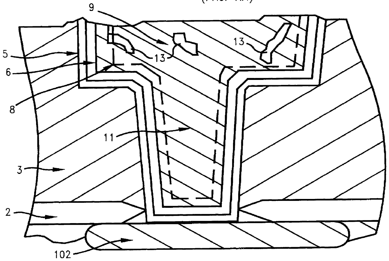
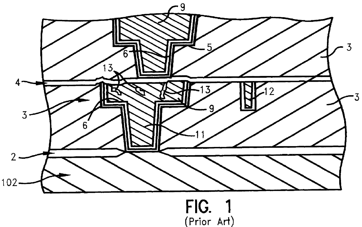
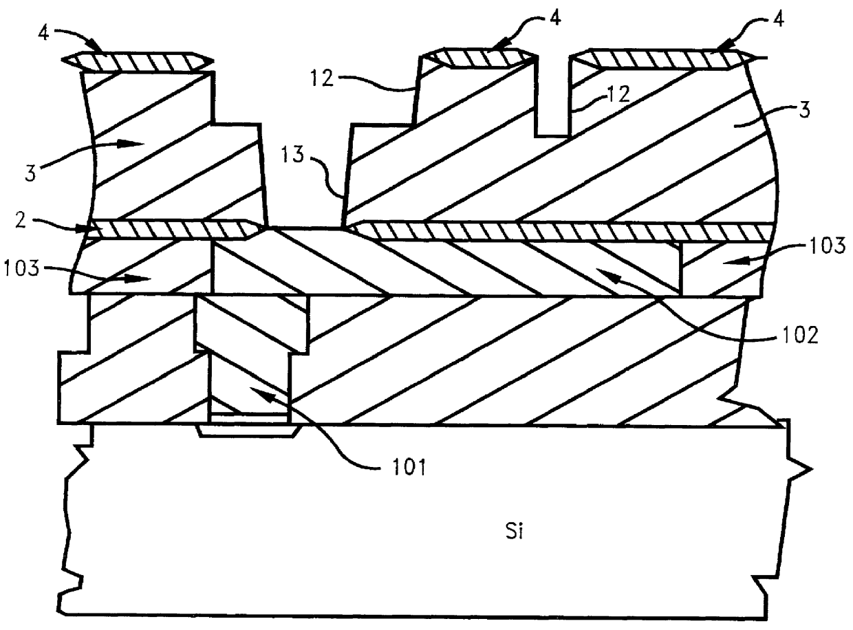
Referring to FIG. 2, there is shown a cross-section of conventional silicon semiconductor structure comprised of various device contact studs 101 and local interconnects 102, typically tungsten with underlayers of titanium and titanium nitride (not shown). The method of the present invention forms reliable multilevel interconnections of copper lines, at sub-micron pitch, and isolated from one another by low dielectric insulation, making contacts to electrical features in a substrate. The substrate structure may be a semiconductor having plurality of electronic devices, an organic circuit carrier, or a ceramic circuit carrier. The local interconnects 102 are preferably formed by damascene methods of prior art, with the to...


PUM

PropertyMeasurementUnit
thicknessaaaaaaaaaa
thicknessaaaaaaaaaa
thicknessaaaaaaaaaa

Abstract

A method of providing sub-half-micron copper interconnections with improved electromigration and corrosion resistance. The method includes double damascene using electroplated copper, where the seed layer is converted to an intermetallic layer. A layer of copper intermetallics with halfnium, lanthanum, zirconium or tin, is provided to improve the electromigration resistance and to reduce defect sensitivity. A method is also provided to form a cap atop copper lines, to improve corrosion resistance, which fully covers the surface. Structure and methods are also described to improve the electromigration and corrosion resistance by incorporating carbon atoms in copper intersititial positions.

Description

1. Field of the InventionThe present invention relates to the field of semiconductor manufacturing and, more specifically, to the design of copper based interconnections in sub-micron dimensions with reduced sensitivity for corrosion and defects, and thereby, with improved reliability. The invention also relates to providing methods for forming the designed structure.2. Description of Related ArtAs device geometry continues to scale down for Ultra Large Scale Integrated circuits, there is a growing demand for an interconnect wiring with minimum pitch and high conductivity, and, for a passivation material with a low dielectric constant, while requiring a more robust reliability than ever before.One approach has been to use copper metallurgy, for its high conductivity and high electromigration resistance, along with polyimide passivation for low cross capacitance. A process utilizing this approach is disclosed by Luther et al. in VLSI Multilevel Interconnection Conference (VMIC), pp.1...

Claims


Application Information

Patent Timeline
Patent Type & Authority Patents(United States)
IPC IPC(8): H01L21/768H01L21/70
CPCH01L21/76846H01L21/76847H01L21/76849H01L21/76877H01L21/76867H01L21/76873H01L21/76858
Inventor ASHLEY, LEONDALAL, HORMAZDYAR M.NGUYEN, DU BINHRATHORE, HAZARA S.SMITH, RICHARD G.
Owner GLOBALFOUNDRIES INC
Why Eureka
Try Eureka