
Multilayer varistor

a multi-layer varistor and varistor technology, applied in the field of multi-layer varistor, can solve the problems of short-circuit failure of the capacitor, insufficient surge resistance in some applications, and undesirable values of x greater than 0.4

Inactive Publication Date: 2000-12-12
TDK CORPARATION
View PDF19 Cites 39 Cited by
  • Summary
  • Abstract
  • Description
  • Claims
  • Application Information

AI Technical Summary

Problems solved by technology

This multilayer ceramic capacitor has a high dielectric constant and a high capacitance, but its surge resistance is insufficient in some applications due to the presence of chromium.
In automotive electric circuits, for example, surge voltage often occurs from the motor, spark plugs and static electricity and can cause short-circuit failure of the capacitor.
Values of x greater than 0.4 are undesirable because of a significant drop of dielectric constant in a low temperature region, especially below 0.degree. C.
Values of y greater than 0.4 are undesirable because of a significant drop of dielectric constant in a high temperature region, especially above 100.degree. C.
Too larger sums of x+y would be undesirable because of short sintering and insufficient densification.
Values of z greater than 0.3 are undesirable because of a significant drop of dielectric constant in a high temperature region, especially above 100.degree. C.
Values of m greater than 1.2 or less than 0.9 are undesirable because of short sintering and insufficient densification.
A too low content of SiO.sub.2 +Al.sub.2 O.sub.3 would fail to provide nonlinear voltage-current characteristics, that is, varistor characteristics.
A too high content of SiO.sub.2 +Al.sub.2 O.sub.3 would cause a significant drop of dielectric constant.
If the sum of the contents of the respective oxides is greater than 5%, there would occur drastic lowering of sinterability and insufficient densification, resulting in poor insulation resistance and a low dielectric constant.
With too thick ceramic layers, only a low capacitance is available per unit volume and it is difficult to find a compromise between size reduction and performance improvement.
Too thin ceramic layers would lead to low insulation resistance at an applied voltage lower than the varistor voltage.
At an oxygen partial pressure below the range, the conductor of the internal electrode layers can be abnormally sintered and disconnected.
Lower holding temperatures below the range would provide insufficient densification whereas higher holding temperatures beyond the range can lead to inconsistent performance due to discontinuous grain growth and a greater change of capacitance with time upon application of a DC electric field.

Method used


Image

  • Multilayer varistor

Examples


example 1

Multilayer varistors as reported in Tables 1 and 2 were fabricated according to the following procedure. The following pastes were first prepared.

Ceramic laver-forming paste

A raw dielectric material was prepared by wet milling powder ingredients in a ball mill for 16 hours and spray drying the mixture. The powder ingredients were mixed in the proportion shown in Table 1. The ingredients used as the main component were BaTiO.sub.3, BaCO.sub.3, CaCO.sub.3, SrCO.sub.3, and ZrO.sub.2 having a mean particle size of 0.5 .mu.m. Oxide and non-oxide ingredients were used as the subordinate component, with the non-oxide ingredients being MnCO.sub.3 and MgCO.sub.3.

A paste was prepared by milling 100 parts of each raw dielectric material, 5 parts of an acrylic resin, 50 parts of methylene chloride, 20 parts of ethyl acetate, 6 parts of mineral spirit, and 4 parts of acetone in a ball mill.

Internal electrode layer-forming paste

A paste was prepared by milling 100 parts of nickel particles having ...

example 2

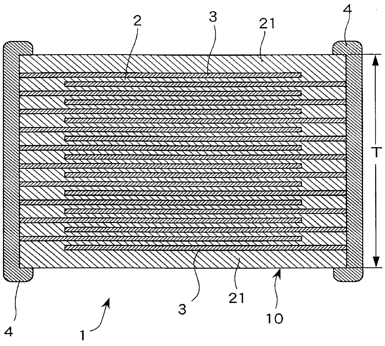
Multilayer varistor samples were prepared as in sample No. 5 of Example 1 except that the thickness and the number of ceramic layers stacked were changed as shown in Table 3. Sample No. 19 had a total thickness T of 1.5 mm. Similar tests were made on these samples, with the results shown in Table 3. For ease of comparison, the results of sample No. 5 are also shown in Table 3.

As is evident from Table 3, sample No. 18 having ceramic layers of more than 25 .mu.m thick has a sufficient maximum peak current, but a low capacitance and an extremely increased value of V.sub.0.1. It is then less effective for noise suppression.

example 3

Multilayer varistor samples were prepared as in Example 1 except that ceramic layers had a thickness of 3 .mu.m and the number of ceramic layers stacked was 2 so that the resultant samples had a lower capacitance than the samples of Example 1. The ceramic layers had a composition as shown in Tables 4 and 6. Nickel particles with a mean particle size of 0.4 .mu.m were used in the internal electrode layer-forming paste and the thickness of the internal electrode layer was changed to 1.5 .mu.m. Other changes included a holding temperature of 240.degree. C. among the binder removal conditions; a holding temperature of 1,260.degree. C. and an oxygen partial pressure of 1.times.10.sup.-11 atm. among the firing conditions; and an oxygen partial pressure of 1.times.10.sup.-6 atm. among the annealing conditions. For sample Nos. 62 and 63 in Table 6, ceramic layers had a thickness of 25 .mu.m.

These samples were tested as in Example 1 except for measurement of insulation resistance. The result...


PUM

PropertyMeasurementUnit
Percent by massaaaaaaaaaa
Volumeaaaaaaaaaa
Volumeaaaaaaaaaa

Abstract

A multilayer varistor comprising a varistor chip body having alternately stacked ceramic layers and internal electrode layers is provided. The ceramic layer is composed of a composite oxide containing Ti and / or Zr and Ba as a main component and Si and / or Al as a subordinate component, substantially free of Cr, and has a perovskite phase. The internal electrode layer is composed of a conductor containing a base metal such as Ni or Ni alloy as a main component. The varistor is used in an electric circuit for suppressing noise.

Description

1. Field of the InventionThis invention relates to a multilayer varistor of the structure wherein ceramic layers having varistor characteristics are stacked between internal electrode layers.2. Prior ArtVaristors are utilized in low-voltage electronic equipment for absorbing high-voltage pulsative noise while bypass capacitors are utilized for removing low-voltage and high-frequency alternating noise. An advanced device having both the functions is a ceramic capacitor with varistor performance. A multilayer structure was proposed for the ceramic capacitor for reducing its size without detracting from its capacitance and reliability as disclosed in Japanese Patent Application Kokai (JP-A) Nos. 82386 / 1993, 275270 / 1993, 176954 / 1994, and 340472 / 1994.JP-A 82386 / 1993, 275270 / 1993, and 176954 / 1994 disclose grain boundary insulated semiconductor ceramics based on SrTiO.sub.3, which cannot fully remove alternating noise and are less effective in suppressing the rise of pulsative noise since ...

Claims


Application Information

Patent Timeline
IPC IPC(8): H01C7/115H01C7/105
CPCC04B35/4682H01C7/115C04B35/638C04B35/49C04B2235/3206C04B2235/3208C04B2235/3213C04B2235/3215C04B2235/3217C04B2235/3224C04B2235/3225C04B2235/3227C04B2235/3229C04B2235/3241C04B2235/3251C04B2235/3258C04B2235/3262C04B2235/3272C04B2235/3275C04B2235/3279C04B2235/3281C04B2235/3284C04B2235/3293C04B2235/3294C04B2235/3296C04B2235/3298C04B2235/3418C04B2235/6562C04B2235/6565C04B2235/6567C04B2235/6582C04B2235/6584C04B2235/6588C04B2235/663C04B2235/72C04B2235/768
Inventor ARASHI, TOMOHIRONAKANO, YUKIEHITOMI, ATSUSHISATO, AKIRANOMURA, TAKESHI
Owner TDK CORPARATION
Learn More