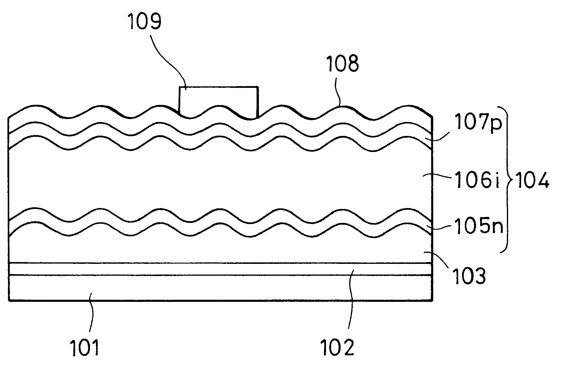
Photovoltaic cell
- Summary
- Abstract
- Description
- Claims
- Application Information
AI Technical Summary
Benefits of technology
Problems solved by technology
Method used
Image

Examples
experiment 1
[ Addition of Titanium]
Samples 1a, 1b, 1c, 1d and 1e were prepared by depositing Al--Ti alloys containing 0.5, 2, 4, 5 and 6 atomic percent of Ti at a thickness of 7,500 .ANG. on a mirror-polished glass plate 7059 made by Corning Incorporated by DC magnetron sputtering. A Ti chip having a purity of 99.999% and a size of 5 mm by 5 mm by 1 mm was placed on the Al target so as to achieve the given compositions in Samples 1a through 1e. Sample 1f having a pure aluminum film was prepared using Al having a purity of 99.999% as a target in the same manner for comparison. Since these films were deposited at a rate of 40 .ANG. / sec at room temperature on a specular substrate, the surface of the deposited film was also specular. All the samples other than Sample 1f were analyzed with an energy dispersion x-ray micro analyzer (XMA) to determine their compositions.
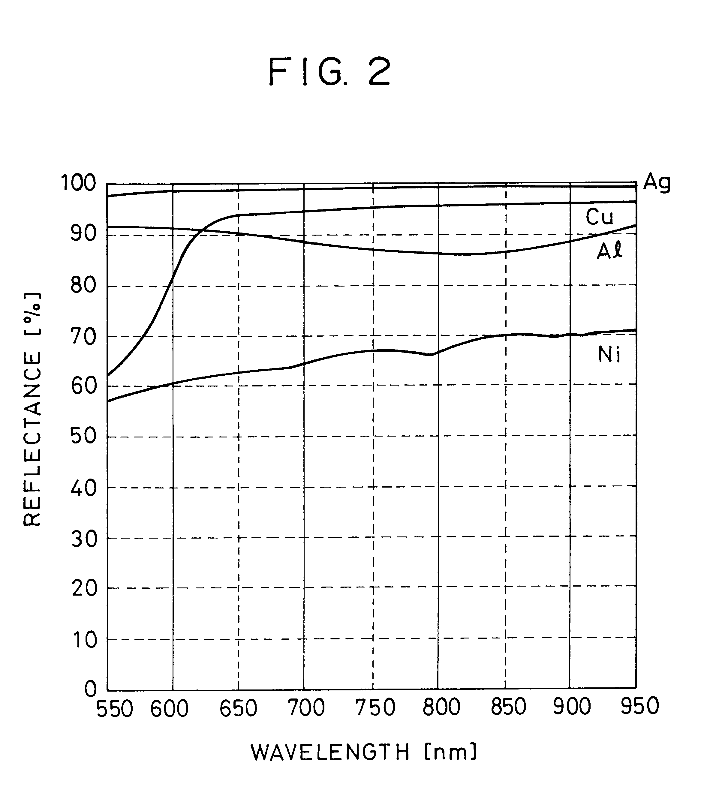
Reflectance of these samples over a wavelength range from 400 to 1,200 nm was determined. Since Al has a local minimum reflectance at...
experiment 2
[ Addition of Magnesium]
Samples 2a, 2b, 2c, 2d and 2e were prepared by depositing Al--Mg alloys containing 0.5, 1, 3, 5 and 8 atomic percent of Mg at a thickness of 7,500 .ANG. on the mirror-polished glass plate set forth in Experiment 1 by the same process as in Experiment 1. Reflectance of these samples over a wavelength range from 400 to 1,200 nm was determined. Reflectance at 830 nm as a typical value is set forth in FIG. 8. FIG. 8 demonstrates that the reflectance of the Al--Mg film at 830 nm is improved by addition of 5 atomic percent or less of Mg as in the case of the addition of Ti. A diffraction pattern of Sample 2b has a strong (111) peak which is approximately 3.6 times that of the (200) peak and no (220) and (311) peaks, suggesting predominant orientation of the (111) plane.
experiment 3
[ Addition of Silver]
Samples 3a, 3b, 3c, 3d and 3e were prepared by depositing Al--Ag alloys containing 3, 8, 12, 20 and 28 atomic percent of Ag at a thickness of 7,500 .ANG. on the mirror-polished glass plate set forth in Experiment 1 by the same process as in Experiment 1. Sample 3f having a pure Ag film was also prepared for comparison. Reflectance of these samples over a wavelength range from 400 to 1,200 nm was determined. Reflectance at 830 nm as a typical value is set forth in FIG. 7. FIG. 7 demonstrates that the reflectance of the Al--Ag film at 830 nm is improved as in the case of the Al--Ti film and exhibits a maximum value at near 10 atomic percent of Ag. Preferably, the Ag content is 25 atomic percent or less. A diffraction pattern of Sample 3d containing 12 atomic percent of Ag has a unique (111) peak at the same angle 2.theta. as the (111) peak in Sample 1b, suggesting predominant orientation of the (111) plane.
PUM
 Abstract
Description
Claims
Application Information
 - R&D
- Intellectual Property
- Life Sciences
- Materials
- Tech Scout
- Unparalleled Data Quality
- Higher Quality Content
- 60% Fewer Hallucinations
Browse by: Latest US Patents, China's latest patents, Technical Efficacy Thesaurus, Application Domain, Technology Topic, Popular Technical Reports.
© 2025 PatSnap. All rights reserved.Legal|Privacy policy|Modern Slavery Act Transparency Statement|Sitemap|About US| Contact US: help@patsnap.com