Method of silicon oxide and silicon glass films deposition

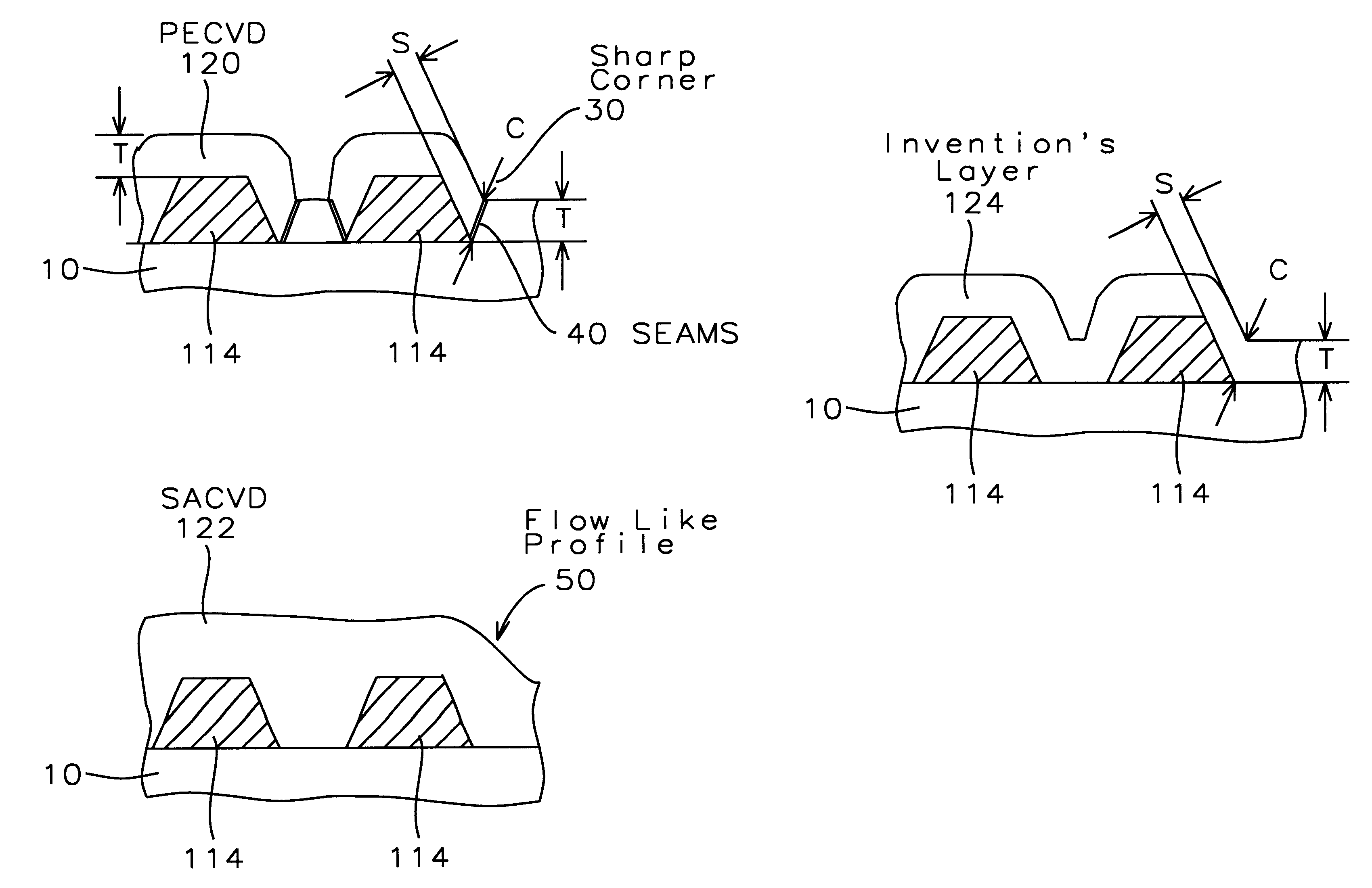
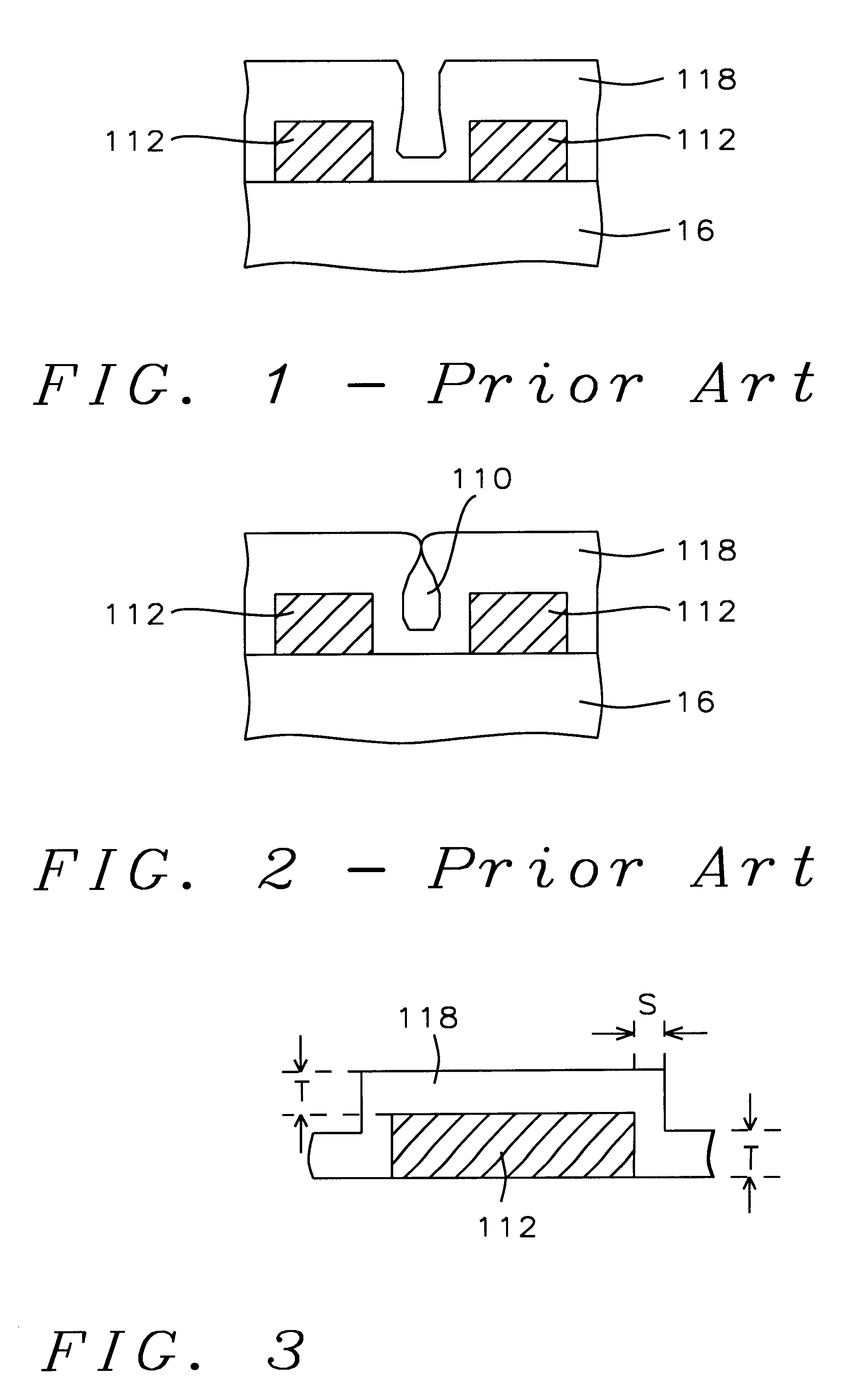
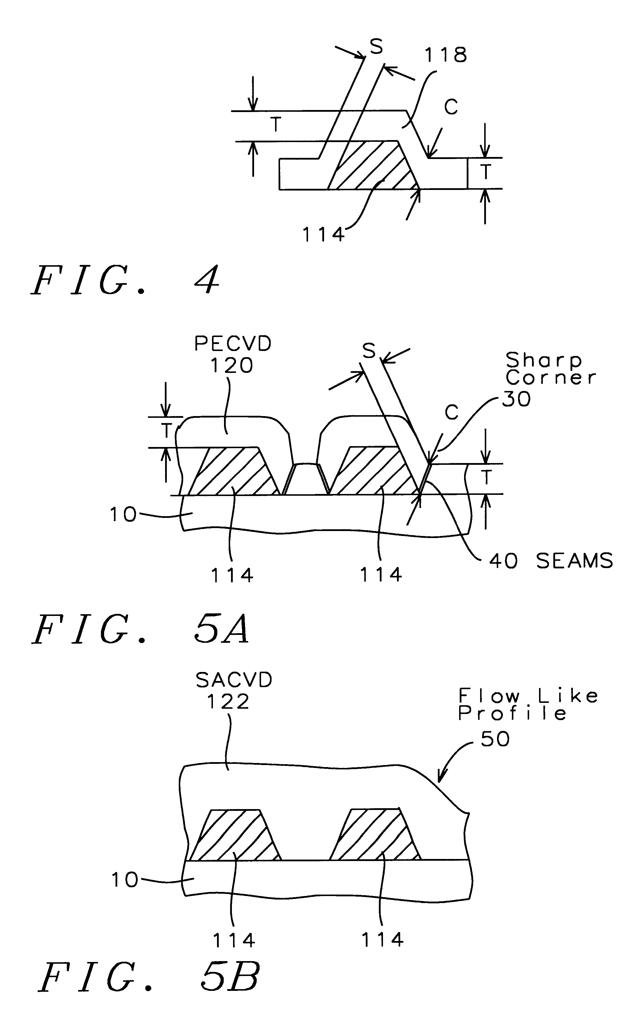
a technology of silicon glass and silicon oxide, which is applied in the direction of chemical vapor deposition coating, coating, electrical equipment, etc., can solve the problems of voids such as shown in fig. 2, unsatisfactory, and irregular coatings such as shown in fig. 1, and achieve the effect of improving film integrity and step coverag

Inactive Publication Date: 2001-03-06
CHARTERED SEMICONDUCTOR MANUFACTURING
View PDF6 Cites 294 Cited by
  • Summary
  • Abstract
  • Description
  • Claims
  • Application Information

AI Technical Summary

Benefits of technology

The invention has the following advantages: stationery deposition rate; no surface sensitivity; improvement of step coverage; rounding of bottom corners--improvement of film inte

Problems solved by technology

An irregular coating such as shown in FIG. 1 is, in many situations, unacceptable because a non-planar surface degrades the resolution of subsequent photolithography.
Voids such as shown in FIG. 2 are even less desirable because etching and dielectric properties will be non-uniform.

Method used


Image

  • Method of silicon oxide and silicon glass films deposition
  • Method of silicon oxide and silicon glass films deposition
  • Method of silicon oxide and silicon glass films deposition

Examples


Embodiment Construction

The present invention will be described in detail with reference to the accompanying drawings. In the following description numerous specific details are set forth such as flow rates, pressure settings, thickness, etc., in order to provide a more thorough understanding of the present invention. It will be obvious, however to one skilled in the art that the present invention may be practiced without these details. In other instances, well known process have not been described in detail in order to not unnecessary obscure the present invention. Also, the flow rates in the specification can be scaled up or down keeping the same molar % or ratios to accommodate difference sized reactors as is known to those skilled in the art. Likewise the other process parameters for the invention's processes can be scaled up or down depending on the specifications of the reactor and requirement of future technology products.

I. Background

A. Measurement of Oxide Layer Conformance

Conformance can be measu...


PUM

PropertyMeasurementUnit
Pressureaaaaaaaaaa
Pressureaaaaaaaaaa
Pressureaaaaaaaaaa

Abstract

A method for fabricating a silicon oxide and silicon glass layers at low temperature using soft power-optimized Plasma-Activated CVD with a TEOS-ozone-oxygen reaction gas mixture (TEOS O3/O2 PACVD) is described. It combines advantages of both low temperature Plasma-Enhanced Chemical Vapor Deposition (PECVD) and TEOS-ozone Sub-Atmospheric Chemical Vapor Deposition (SACVD) and yields a coating of silicon oxide with stable and high deposition rate, no surface sensitivity, good film properties, conformal step coverage and good gap-fill. Key features of the invention's O3/O2 PACVD process are: a plasma is maintain throughout the entire deposition step in a parallel plate type reactor chamber, the precise RF plasma density, ozone concentration in oxygen and the deposition temperature. These features provide the reaction conditions for the proper O3/O2 reaction mechanism that deposits a conformal silicon oxide layer. The process has significant implication for semiconductor device manufacturing involving the deposition of a dielectric over a conducting non-planar surface.

Description

1. Field of the InventionThis invention relates generally to fabrication of semiconductor devices and more particularly to the fabrication of a silicon oxide and silicon glass deposition using a combined power-optimized Plasma-Activated CVD with tetraethoxysilane-ozone-oxygen reaction gas mixture (TEOS-O.sub.3 / O.sub.2 PACVD).2. Description of the Prior ArtIn the fabrication of devices such as semiconductor devices, a variety of material layers is sequentially formed and processed on the substrate. (For the purpose of this disclosure, the substrate includes a bulk material such as semiconductor, e.g., silicon, body, and if present, various regions of materials such as dielectric materials, conducting materials, metallic materials, and / or semiconductor materials). Often, one of the material regions utilized in this fabrication procedure includes a silicon oxide, i.e., a material nominally represented by the formula SiO.sub.n, where n=.about.2. For example, silicon oxide regions are u...

Claims


Application Information

Patent Timeline
IPC IPC(8): C23C16/40H01L21/02H01L21/316
CPCC23C16/402H01L21/02131H01L21/02164H01L21/02274H01L21/02304H01L21/02362H01L21/31612
Inventor VASSILIEV, VLADISLAV
Owner CHARTERED SEMICONDUCTOR MANUFACTURING
Why Eureka
Try Eureka