

Integrated circuit and method
a technology of integrated circuits and circuits, applied in the field of integrated circuits and methods, can solve the problems of manufacturing problems of memory with these new dielectrics
- Summary
- Abstract
- Description
- Claims
- Application Information
AI Technical Summary
Benefits of technology
Problems solved by technology
Method used
Image

Examples
first preferred embodiments
FIGS. 3a-o illustrate in cross sectional elevation views the steps of first preferred embodiment fabrication methods for integrated circuits (e.g., CMOS or BiCMOS) with capacitors or memory cells (e.g., DRAM or FeRAM cells) as follows.
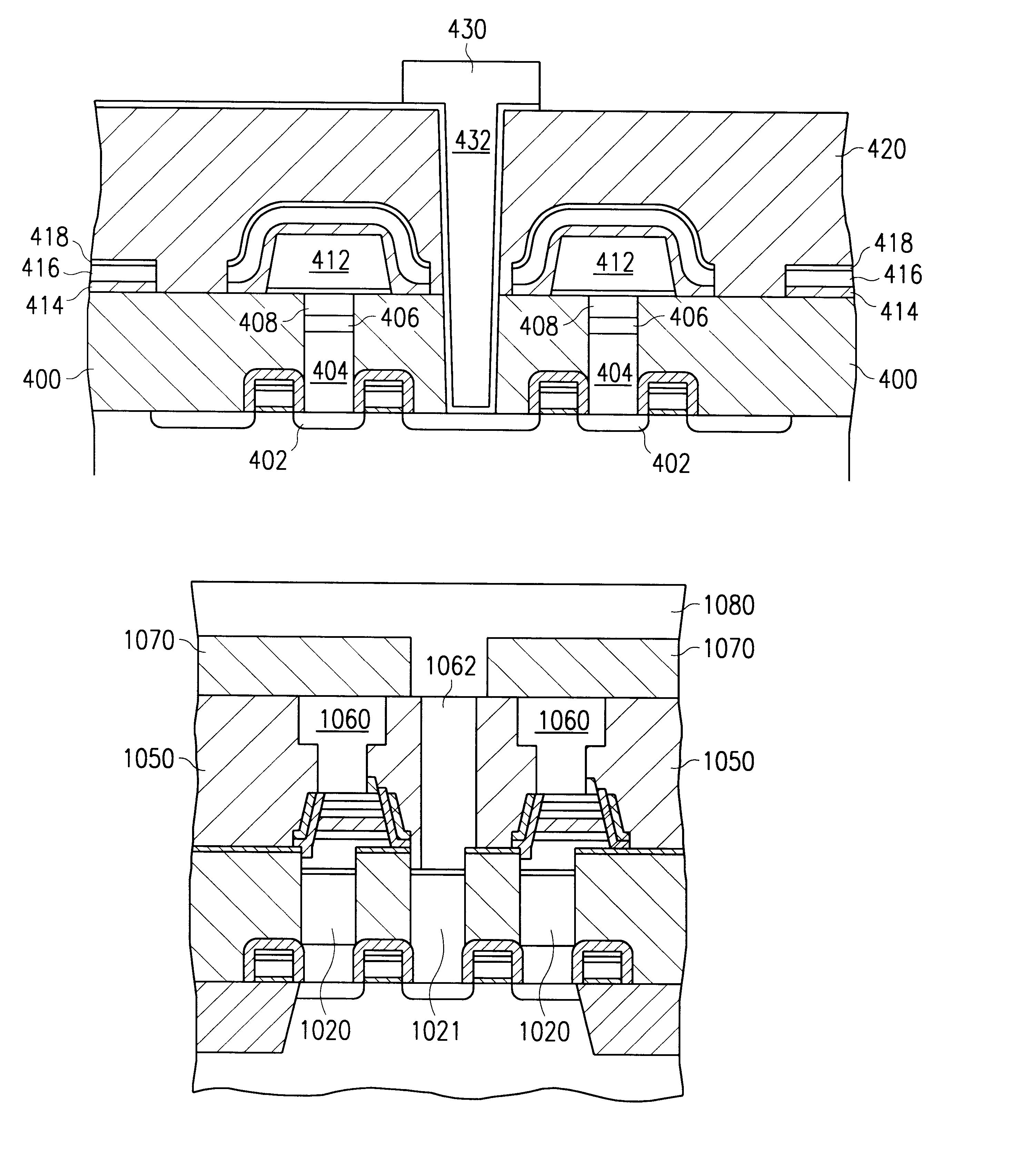
(1) Start with a silicon wafer (or silicon on insulator wafer) with shallow trench isolation and twin wells for CMOS devices. Perform threshold adjustment implants (which may differ for cell transistors and various peripheral transistors), and form gate dielectric. Deposit tungsten silicide coated polysilicon gate material and a silicon dioxide layer, then pattern the layers to form oxide-topped gates plus gate level interconnects. The gate material could also provide a polysilicon emitter for bipolar devices which would also require a prior base implant. See FIG. 3a which shows silicon substrate 300 with shallow trench isolation oxide 302 plus gate dielectric 304, gates 306, and gate level interconnect 307 (i.e., wordlines for a memory array). Gates 3...
second preferred embodiments
FIGS. 6a-o illustrate in cross sectional elevation views the steps of second preferred embodiment fabrication methods for integrated circuits (e.g., CMOS or BiCMOS) with memory cells (e.g., FeRAM cells) as follows.
(1) Follow steps (1)-(7) of the foregoing first preferred embodiments to have a structure as illustrated in FIG. 3e. Optionally, dielectric 318 includes a 30 nm thick top layer 602 to act as a diffusion barrier. Layer 602 could be TiO2, Al203, and so forth.
(2) Form a stack of layers as follows:
Sputter deposit 50 nm thick layer 604 of Tio.sub.0.6 Al.sub.0.4 N (bottom conducting diffusion barrier);
Sputter deposit 100 nm thick layer 606 of Ir (bottom electrode, Pt is not as good as Ir for PZT);
MOCVD 100 nm thick layer 608 of PZT (ferroelectric);
Sputter deposit 50 nm thick layer 610 of Ir (top electrode), additionally, a 10 nm thick layer 612 of IrO2 may be included;
Sputter deposit 50 nm thick layer 614 of Ti.sub.0.6 Al.sub.0.4 N (top conducting diffusion barrier); alternative...
third preferred embodiments
FIG. 8 illustrates in cross sectional elevation views the new step of third preferred embodiments methods for fabrication of integrated circuits (e.g., CMOS or BiCMOS) with capacitors or memory cells (e.g., FeRAM cells) as follows.
(1) Follow step (1) of the second preferred embodiments (which is the same as steps (1)-(7) of the first preferred embodiments).
(2) Sputter deposit 30 nm thick layer 802 of Ti.sub.0.6 Al.sub.0.4 N (bottom conducting diffusion barrier) and then sputter deposit 50 nm thick layer 804 of Pt (bottom electrode). Annealing the Pt can increase grain size and modify subsequent SBT characteristics.
(3) [26218] Load Pt 804 with bismuth by spin coating 5 ml (for a 6 inch wafer) of a 0.04M solution 806 of Bi(OAc)3 in a mixture of pyridine and acetic acid (ratio of pyridine to acetic acid of 1 to 2.9 by weight) and drying at 300 C. for 5 minutes. Then diffuse Bi into the surface region of the Pt by firing at 700 C. for 60 minutes; see FIG. 8. The firing time will determi...
PUM
 Abstract
Description
Claims
Application Information