Optical probe for detecting or irradiating light and near-field optical microscope having such probe and manufacturing method of such probe

a manufacturing method and optical probe technology, applied in the direction of scanning probe techniques, instruments, material analysis through optical means, etc., can solve the problems of degrading the resolution of the microscope, difficult to produce a plurality of fine optical probes in an integrated fashion, and difficult to arrange a plurality of optical probes in an array

Inactive Publication Date: 2001-04-10
CANON KK
View PDF5 Cites 167 Cited by
  • Summary
  • Abstract
  • Description
  • Claims
  • Application Information

AI Technical Summary

Problems solved by technology

However, if no micro-aperture is formed in the optical probe as described above by referring to the PSTM, the probe will detect not only evanescent light but also stray light scattered by the undulations of the surface of the specimen to consequently degrade the resolution of the microscope.
It is difficult to produce a plurality of fine optical probes in an integrated fashion by the known technique of etching an optical fiber.
It is also difficult to arrange a plurality of optical probes in an array in order to improve the detection speed of the PSTM.
Additionally, when an optical fiber is used for the SNOM or the PSTM, it has to be aligned with the optical axis of the light emitting device or the light receiving device which also makes it difficult to arrange optical probes in an array.
Then, it is very difficult to densely arrange a large number of optical probes.
Then, the size of the minimal possible aperture that can be produced with such a technique will be 100 nm at most and it is practically impossible to produce a micro-aperture as small as 10 nm.
Therefore, the resolution of the SNOM is inevitably limited by the above technical limitation.
Additionally, this technique is time consuming and costly because it is complicated and involves complex processing steps.
While it is theoretically possible to form a micro-aperture smaller than 100 nm by means of an electron beam processing apparatus or a focused ion beam processing apparatus, the use of such an apparatus entails an aligning process that has to be controlled in a complicated manner and a problem of dimensional irregularity of the produced optical probes.

Method used


Image

  • Optical probe for detecting or irradiating light and near-field optical microscope having such probe and manufacturing method of such probe
  • Optical probe for detecting or irradiating light and near-field optical microscope having such probe and manufacturing method of such probe
  • Optical probe for detecting or irradiating light and near-field optical microscope having such probe and manufacturing method of such probe

Examples


example 2

In Example 2, a total of 100 micro-apertures arranged in a 10.times.10 matrix were prepared for optical probes as described above by referring to Example 1. The micro-apertures were observed through a scanning electron microscope to find that their diameters were between 10 and 30 nm. The surface of the substrate were etched uniformly by forming silicon dioxide on the substrate surface, using oxidizing gas, and sacrificially etching the silicon dioxide by means of hydrofluoric acid solution.

example 3

In Example 3, an optical probe unit having light irradiating means was prepared in a manner as described below.

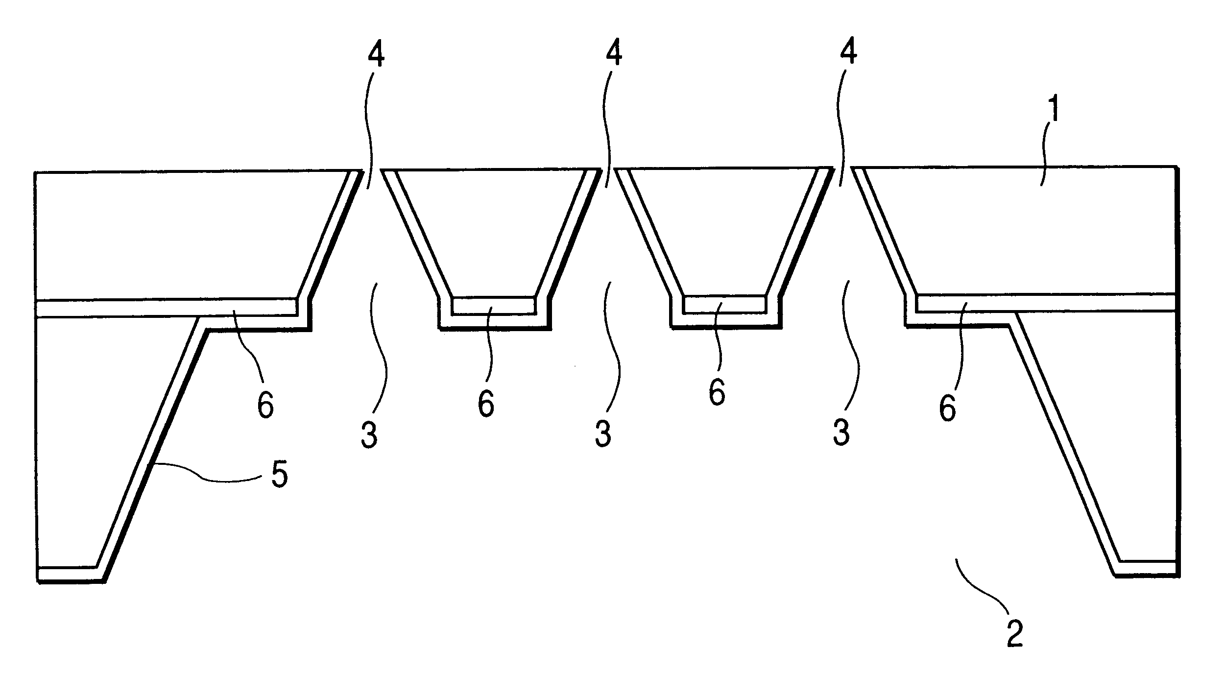
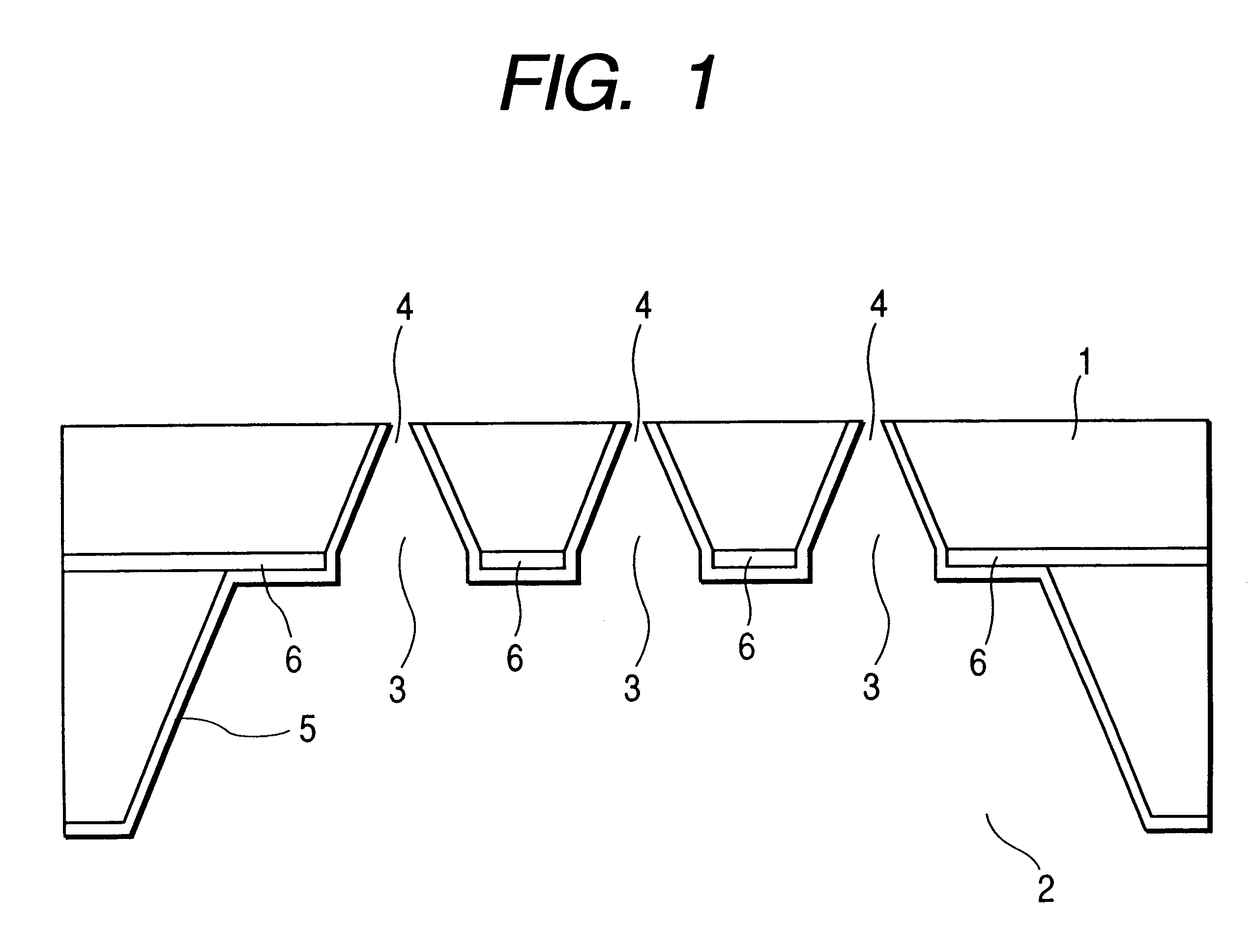
FIG. 4 is a schematic cross sectional view of part of an information recording apparatus according to the invention and having a plurality of micro-apertures for so many optical probes provided with respective light irradiating means. The optical probe unit was used as optical recording head of an opto-magnetic recording system. Referring to FIG. 4, reference numerals 701, 702 and 703 denote probes #1, #2 and #3 respectively comprising micro-apertures the same as those prepared in Example 1 above. Laser beams 711, 712 and 713 emitted from respective surface light emitting lasers 721, 722, 723 of a surface light emitting laser array 720 arranged on a single substrate and fitted to the recess of the optical probe unit as light irradiating means seep out from respective probes #1, #2 and #3 as evanescent lights #1 (741), #2 (742) and #3 (743). Partitions 724 were arranged betw...

example 4

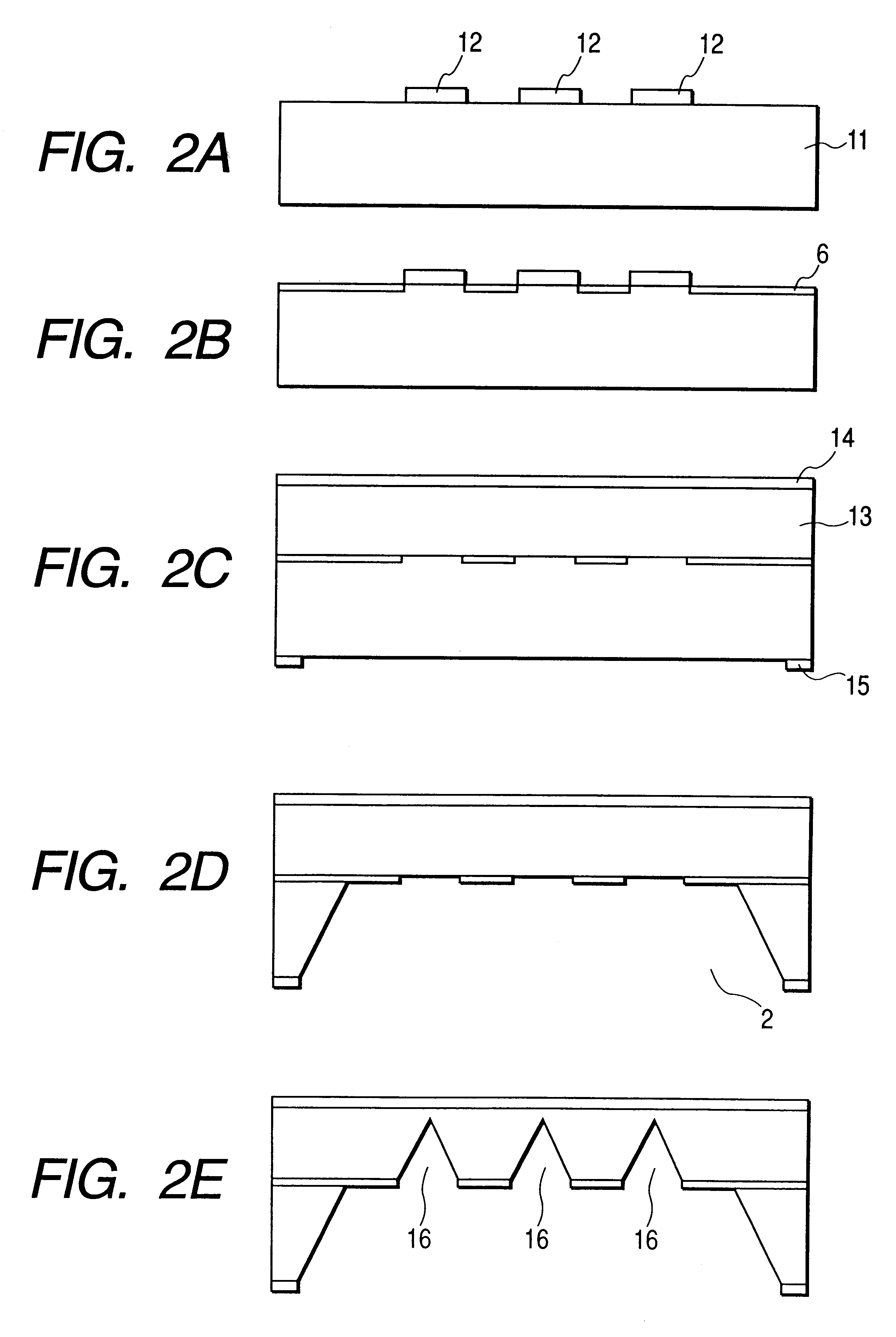
This example represents a second mode of carrying out the method of manufacturing optical probes according to the invention. FIGS. 5A through 5G are schematic cross sectional views of optical probes being prepared by the second mode of carrying out the invention, showing different manufacturing steps.

The manufacturing process of this example will be described below.

A pattern of photoresist 32 as shown in FIG. 5A was formed on a 525 .mu.m thick silicon substrate 31 having a planar orientation of plane and a resistivity of 1 to 10 .OMEGA.cm by using a photolithography process. The pattern had a size of 20 .mu.m square.

Then, phosphor (P) ions were implanted into the surface of the silicon substrate by means of an ion implanter, using the photoresist 32 as mask. After removing the photoresist, an n-type diffusion layer having an impurity concentration of 1.times.10.sup.18 cm.sup.-3 was formed for the etching stop layer 26 by thermal diffusion (FIG. 5B).

A pn-junction was formed on the in...


PUM

PropertyMeasurementUnit
diameteraaaaaaaaaa
sizeaaaaaaaaaa
sizeaaaaaaaaaa

Abstract

An optical prove for detecting or irradiating evanescent light is manufactured by forming a film having a regulated film thickness on a substrate, then forming a recess from the rear surface of the substrate, and forming a through hole in the film from the side of the recess by etching. The obtained optical probe has a micro-aperture at the tip of the through hole and usually, a plurality of optical probes each having a micro-aperture of uniform profile are formed on a single substrate. In the recess, light-receiving or light-irradiating means may be provided.

Description

1. Field of the InventionThis invention relates to an optical probe for detecting or irradiating evanescent light to be used for a near-field optical microscope. It also relates to a method of manufacturing such an optical probe.2. Related Background ArtThe recent development of the scanning tunneling microscope adapted for direct observation of the electron structure of surface atoms of a conductor has made it possible to visually observe an image of the real space of a specimen with an enhanced degree of resolution regardless of whether the specimen is monocrystalline or noncrystalline (G. Binnig et al., Phys. Rev. Lett. 49, 57 (1983)). Since then, research efforts have been paid on the scanning probe microscope (hereinafter referred to as SPM) particularly in an attempt to look into the micro-structures of various materials.SPMs include scanning tunneling microscopes (STMs), atomic force microscopes (AFMs) and magnetic force microscope (MFMS) that are adapted to observe the surfa...

Claims


Application Information

Patent Timeline
Patent Type & Authority Patents(United States)
IPC IPC(8): G12B21/06G12B21/00G01N37/00G01Q60/18G01Q60/22G01Q70/06
CPCB82Y20/00B82Y35/00G01Q60/22Y10S977/862
Inventor YAGI, TAKAYUKIIKEDA, TSUTOMUKURODA, RYOSHIMADA, YASUHIRO
Owner CANON KK
Why Eureka
Try Eureka