

Active matrix electro-luminescent display thin film transistor
a technology of active matrix and electroluminescent display, which is applied in the direction of optics, instruments, and semiconductor/solid-state device details, etc., can solve the problems of insufficient masking function and adversely affecting the operation of thin film transistors
- Summary
- Abstract
- Description
- Claims
- Application Information
AI Technical Summary
Benefits of technology
Problems solved by technology
Method used
Image

Examples
first embodiment
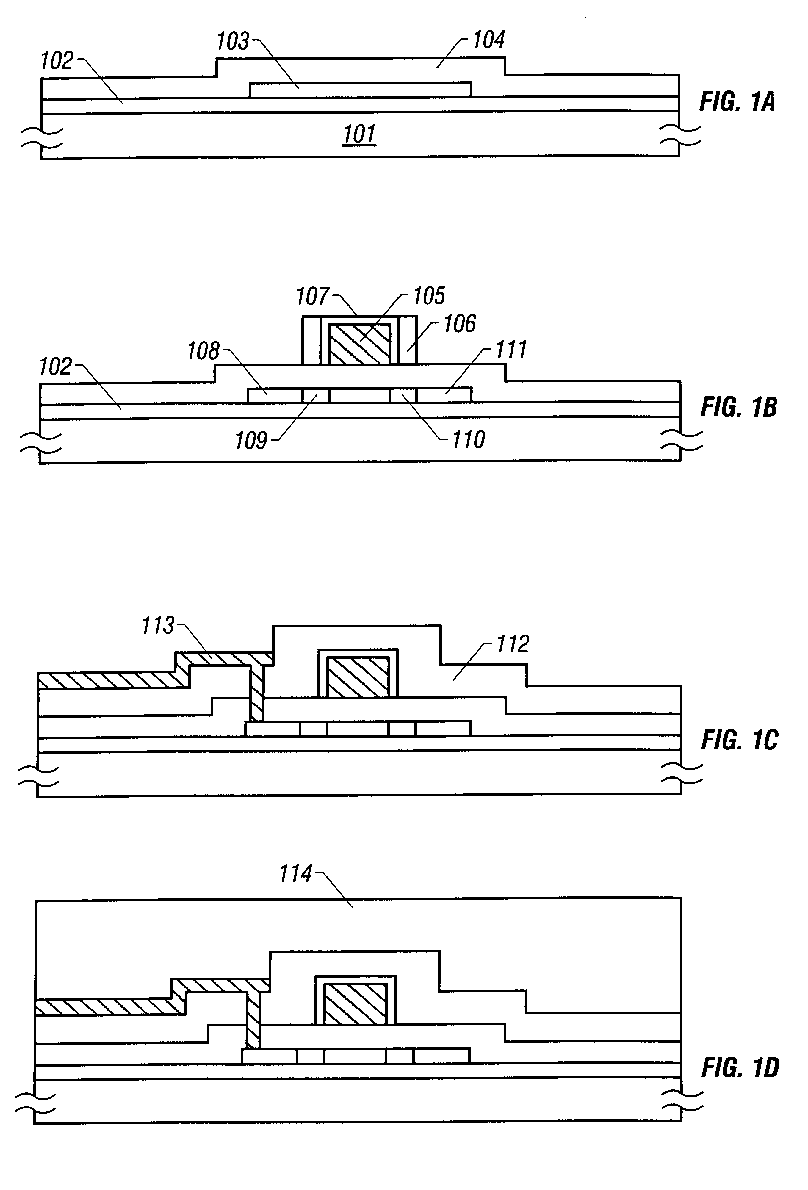
the present invention will now be described. FIGS. 1A through 1D and FIGS. 2A through 2C illustrate steps of producing a pixel portion of an active matrix liquid crystal display to be described in the present embodiment.
As shown in FIG. 1A, a silicon oxide film 102 having a thickness of 3000 .ANG. as a backing film is first formed on a glass substrate 101 using a plasma CVD process.
Next, an amorphous silicon film (not shown) is formed which will later serve as a starting film made of a thin film semiconductor for forming an active later of a thin film transistor. The amorphous silicon film (not shown) is formed to a thickness of 500 .ANG. using a plasma CVD process.
The amorphous silicon film is then crystallized using a heating process or irradiating it with laser beams or using a process which is a combination of the heating process and irradiation with laser beams to obtain a crystalline silicon film (not shown).
The crystalline silicon film (not shown) is patterned to obtain an ac...
second embodiment
the present invention will now be described.
The present embodiment is characterized in that it employs a configuration which is an improvement over the configuration described in the first embodiment to provide higher reliability.
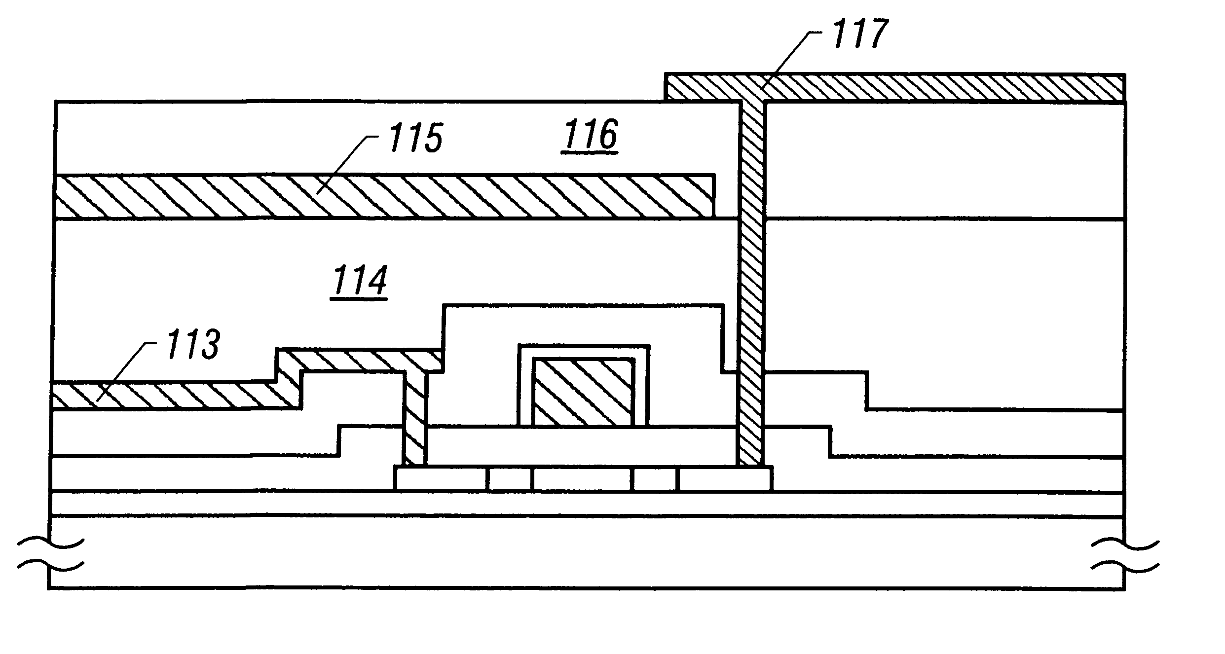
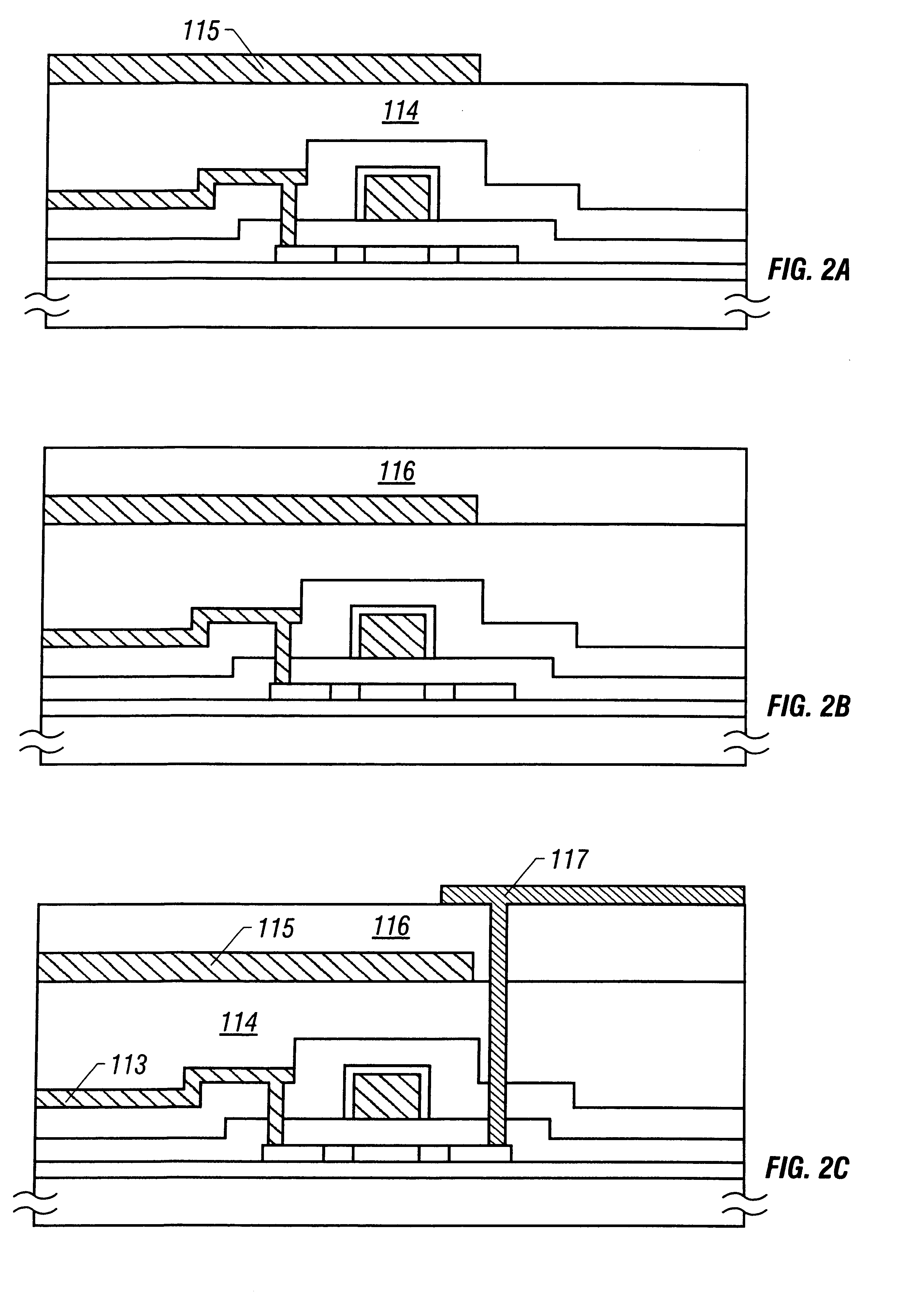
As described above, a metal material such as chromium is used for the masking film and black matrix. From the viewpoint of long term reliability, however, concern exists about dispersion of impurities from the metal material and a short-circuit between the metal material and other electrodes or wiring.
Especially, if there is a pin hole in the layer insulation film 116 in the state as shown in FIG. 2C, a problem arises in that a short-circuit occurs between the masking film 115 (which may simultaneously serve as a black matrix) and the pixel electrode 117.
A possible method for eliminating the influence of a pin hole present in the layer insulation film 116 is to form the layer insulation film 116 as a special multi-layer film.
However, such a method is unfavo...
third embodiment
the present invention will now be described.
The present embodiment relates to a configuration in which an aperture ratio of a pixel is improved. There is a general need for a configuration of a pixel that makes the aperture ratio as large as possible. In order to obtain a large aperture ratio of a pixel, the pixel electrode must be provided to have an area which is as wide as possible.
However, a severe limitation is placed on such an attempt in that if the pixel electrode overlaps the thin film transistor or wiring, a capacity is generated therebetween.
The present embodiment provides a configuration which reduces the problem of generation of a capacity.
FIGS. 4A through 4C show steps of producing the configuration according to the present embodiment. The steps shown in FIGS. 4A and 4B are the same as those in FIGS. 3A and 3B.
First, a masking film 115 made of aluminum is formed as shown in FIG. 4A. An anodic oxide film indicated by 301 is formed on the surface of the masking film 115....
PUM
| Property | Measurement | Unit |
|---|---|---|
| thickness | aaaaa | aaaaa |
| thickness | aaaaa | aaaaa |
| thickness | aaaaa | aaaaa |
Abstract
Description
Claims
Application Information