Method of fabricating Schottky diode and related structure

a diode and diode structure technology, applied in the direction of diodes, semiconductor devices, electrical equipment, etc., can solve the problems of reducing device yield, affecting device performance, and affecting device performance, so as to improve the structure of schottky diodes, reduce the cost of fabrication, and maintain parasitic capacitance low

a diode and diode structure technology, applied in the direction of diodes, semiconductor devices, electrical equipment, etc., can solve the problems of reducing device yield, affecting device performance, and affecting device performance, so as to improve the structure of schottky diodes, reduce the cost of fabrication, and maintain parasitic capacitance low

US6261932B1Inactive Publication Date: 2001-07-17SEMICON COMPONENTS IND LLC

Image

  • Method of fabricating Schottky diode and related structure
  • Method of fabricating Schottky diode and related structure
  • Method of fabricating Schottky diode and related structure

Examples


Embodiment Construction

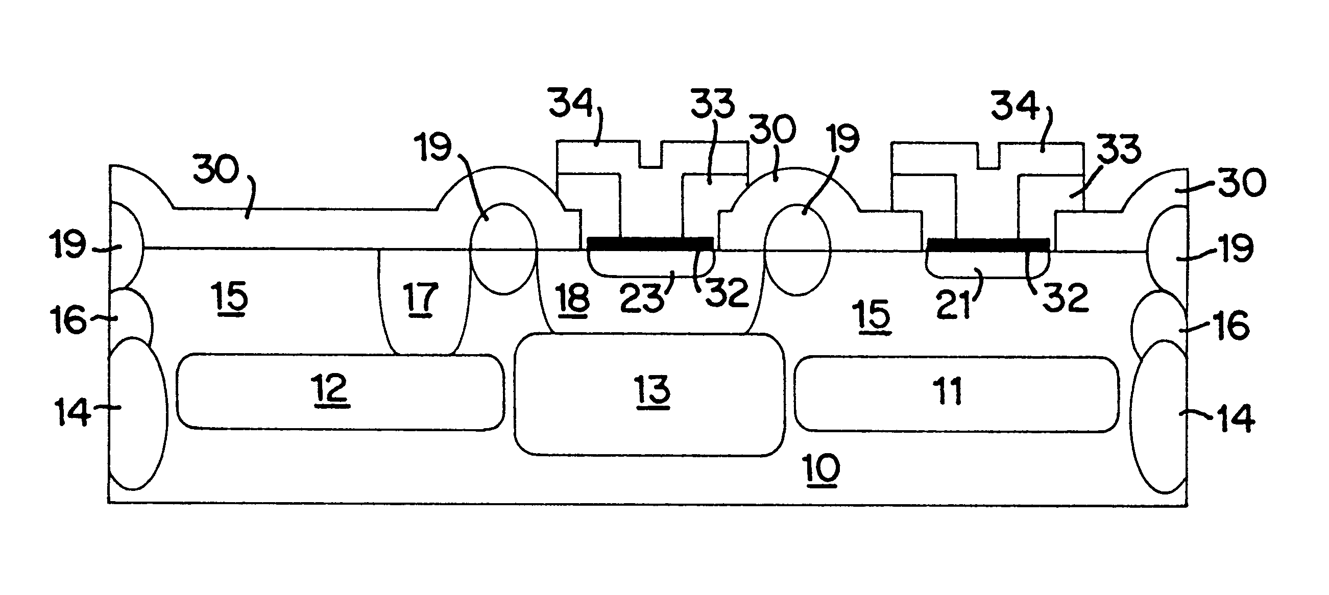
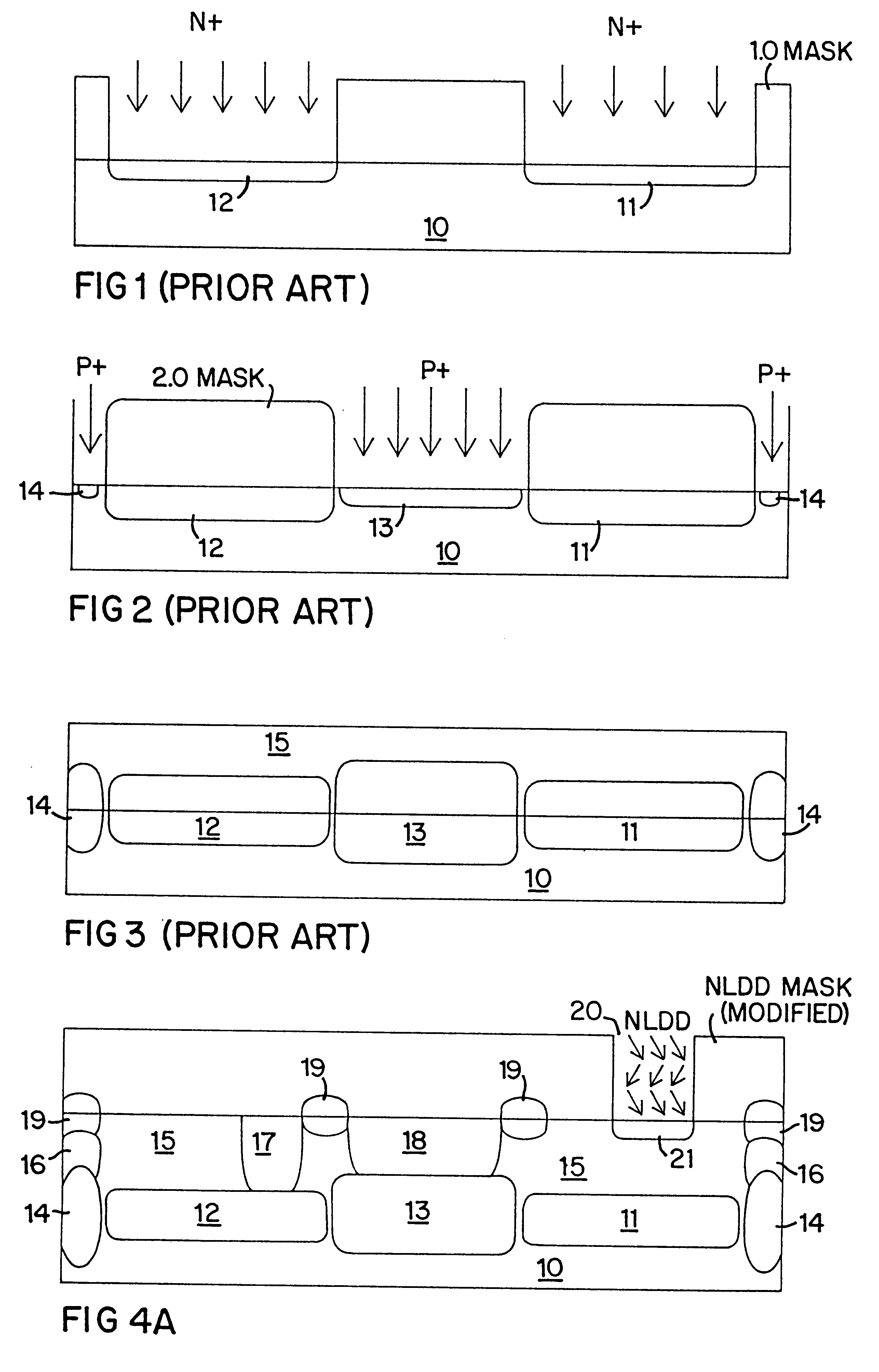
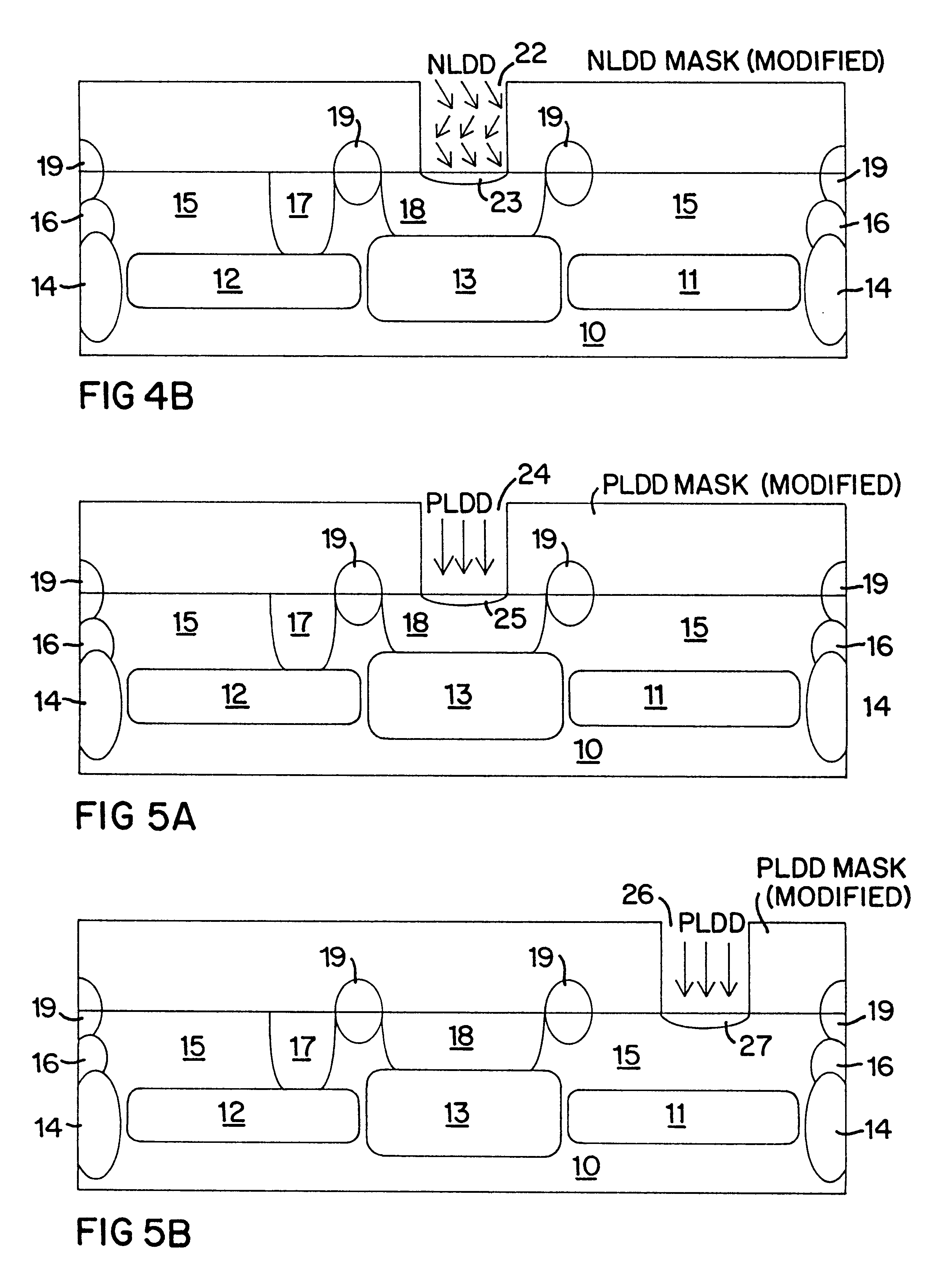
Methods of fabricating several types of improved Schottky diode structures of the present invention at essentially no cost are described in conjunction with a series of key fabrication steps shown in FIGS. 1-7. The fabrication process used to form one or more Schottky diodes may be, and preferably are, integrated into BiCMOS or CMOS fabrication steps previously noted, without adding any new steps. New structures and the relevant mask modifications are shown in FIGS. 4-7. The overall exemplar BICMOS transistor structure mask sequence is the sequence summarized in the Summary of the Invention with modifications as indicated. Of course, alternative fabrication steps may be employed, provided a barrier-modifying layer forms a portion of the Schottky diode between the metal-suicide anode and the doped cathode layer. While the present discussion focuses on the formation of an N-type Schottky diode and the associated N-type epitaxial layer, it is to be understood that similar adjustments i...


PUM


Abstract

A method of forming an improved Schottky diode structure as part of an integrated circuit fabrication process that includes the introduction of a selectable concentration of dopant into the surface of an epitaxial layer so as to form a barrier-modifying surface dopant layer. The epitaxial layer forms the cathode of the Schottky diode and a metal-silicide layer on the surface of the epitaxial layer forms the diode junction. The surface dopant layer positioned between the cathode and the diode junction is designed to raise or lower the barrier height between those two regions either to reduce the threshold turn-on potential of the diode, or to reduce the reverse leakage current of the transistor. The particular dopant conductivity used to form the surface dopant layer is dependent upon the conductivity of the epitaxial layer and the type of metal used to form the metal-silicide junction.

Description

1. Field of the InventionThe present invention relates to methods of fabricating semiconductor devices. In particular, the present invention relates to the steps associated with the fabrication of bipolar, Metal Oxide Semiconductor (MOS), and Bipolar Complementary MOS (BiCMOS) structures. More particularly, the present invention relates to those aspects of the fabrication of BiCMOS structures involving the formation of Schottky diodes of selectable characteristics without modification of the existing fabrication steps. The present invention is a "no cost" method of fabricating improved Schottky diode structures.2. Description of the Prior ArtIn an effort to create increasingly faster semiconductor devices that consume less power, it is a goal in the semiconductor industry to create increasingly smaller integrated circuit (IC) devices. This relates to the interest in creating IC devices requiring lower supply voltages; that is as device power supplies move from a nominal 5.0 volts to...

Claims


Application Information

Patent Timeline
17 Jul 2001
Publication
US6261932B1
IPC
H01L21/02; H01L21/329; H01L29/66; H01L27/06; H01L27/07; H01L29/872; H01L21/8234; H01L29/47
CPC
H01L27/0635; H01L27/0647; H01L29/872; H01L29/66143; H01L27/0766
Inventors
HULFACHOR, RONALD