Organic electroluminescent device

a technology of electroluminescent devices and organic el, which is applied in the direction of discharge tubes/lamp details, luminescent screens of discharge tubes, natural mineral layered products, etc., can solve the problems of low reliability of devices, oxidation resistance, and inability to withstand oxidation

Inactive Publication Date: 2001-10-16
TDK CORPARATION
View PDF13 Cites 33 Cited by
  • Summary
  • Abstract
  • Description
  • Claims
  • Application Information

AI Technical Summary

Problems solved by technology

A problem common to these organic EL devices is reliability.
However, these materials are sensitive to damages during device fabrication, and offer a problem in conjunction with an affinity for electrodes.
However, these materials are susceptible to oxidation and lack stability, and so are a grave factor responsible for a reduction in the service life of the organic EL device and a reliability problem.
A further problem is that the deterioration of an organic thin film is much severer than that of an LED or LD.
Most organic materials are relatively expensive.
However, it is still impossible to obtain an organic EL device superior to prior art organic ELs in terms of emission performance and basic device reliability.

Method used


Image

  • Organic electroluminescent device
  • Organic electroluminescent device
  • Organic electroluminescent device

Examples


first embodiment

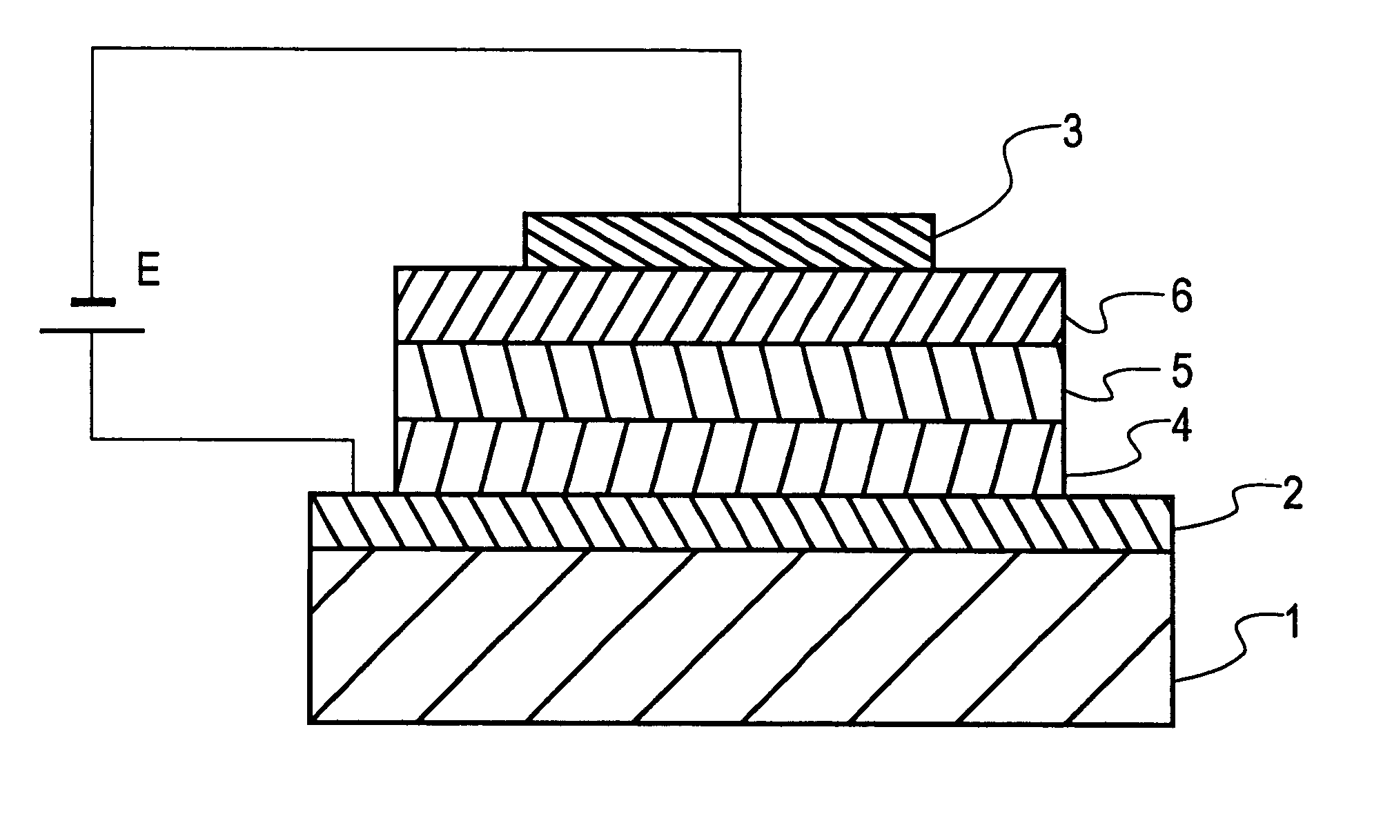
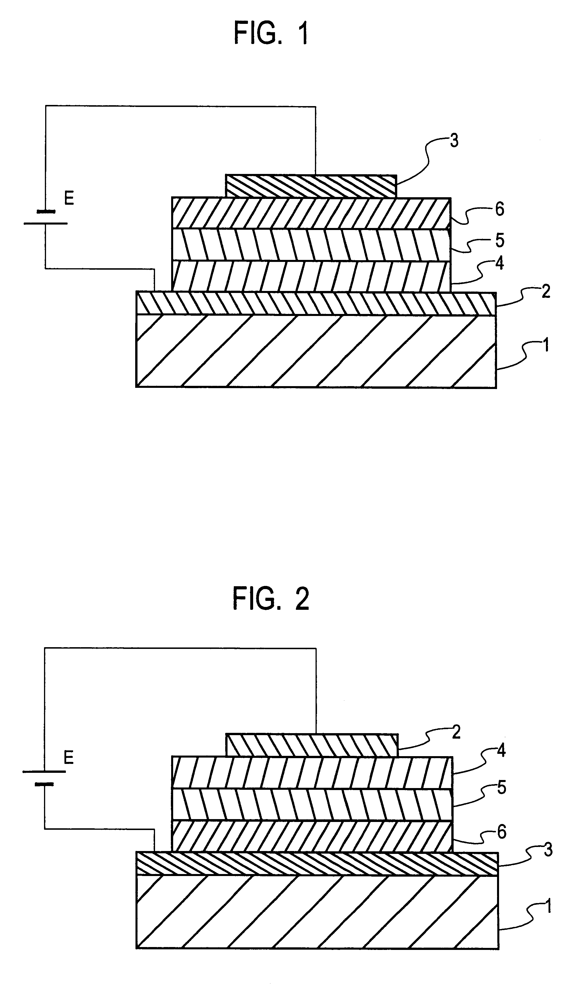
As typically shown in FIG. 1, one embodiment of the organic EL device of the invention comprises, in order from a substrate 1, a hole injecting electrode 2, a hole injecting and transporting layer 4, a light emitting layer 5, an inorganic insulating electron injecting and transporting layer 6 and a cathode 3 which are laminated together on the substrate 1. Another embodiment of the organic EL device of the invention is reversed in multilayer arrangement to the invention (the hole injecting electrode is opposite to the substrate side); it comprises, in order from a substrate 1, a cathode 3, an inorganic insulating electron injecting and transporting layer 6, a light emitting layer 5, a hole injecting and transporting layer 4 and a hole injecting electrode 2 which are laminated together on the substrate 1, as shown in FIG. 2. The reversed multilayer arrangement can prevent damage to the organic layer due to ashing during the formation of the inorganic insulating electron injecting lay...

example 1

A 7059 substrate (made by Corning) used as a glass substrate was scrubbed with neutral detergent. Then, the substrate was fixed to a substrate holder in a sputtering system, where an ITO hole injecting electrode layer was formed by a DC magnetron sputtering process using an ITO oxide target.

The substrate with the ITO film formed on it was ultrasonically washed with neutral detergent, acetone, and ethanol, and then pulled up from boiling ethanol, followed by drying. The substrate was subsequently cleaned on its surface with UV / O.sub.3. Then, the substrate was fixed to the substrate holder in a vacuum evaporation system, which was evacuated to a vacuum of 1.times.10.sup.-4 Pa or lower.

Then, polythiophene was deposited by evaporation at a deposition rate of 0.1 nm / sec. to a thickness of 10 nm thereby forming a hole injecting layer, and TPD was deposited by evaporation at a deposition rate of 0.1 nm / sec. to a thickness of 20 nm thereby forming a hole transporting layer.

With the vacuum k...

example 2

Experiments were carried out as in Example 1 with the exception that the main component, subordinate component and stabilizer in the inorganic insulating electron injecting and transporting layer were changed from SrO to MgO, CaO or an oxide mixture thereof, from Li.sub.2 O to K.sub.2 O, Rb.sub.2 O, K.sub.2 O, Na.sub.2 O, Cs.sub.2 O or an oxide mixture thereof, and from SiO.sub.2 to GeO.sub.2 or an SiO.sub.2 and GeO.sub.2 oxide mixture. The obtained results were much the same as Example 1. The same was also true of when the cathode constituting material was changed from Al to Ag, In, Ti, Cu, Au, Mo, W, Pt, Pd, Ni or an alloy thereof.


PUM

PropertyMeasurementUnit
thicknessaaaaaaaaaa
mol %aaaaaaaaaa
thicknessaaaaaaaaaa

Abstract

An object of the invention is to achieve an organic EL device which has an extended life, weather resistance, high stability, and high efficiency, and is inexpensive as well. This object is accomplished by the provision of an organic EL device comprising a substrate, a pair of a hole injecting electrode and a cathode formed on the substrate, and an organic layer located between these electrodes and taking part in at least a light emission function, wherein between the organic layer and the cathode there is provided an inorganic insulating electron injecting and transporting layer comprising a first component comprising at least one oxide selected from the group consisting of lithium oxide, rubidium oxide, potassium oxide, sodium oxide and cesium oxide, a second component comprising at least one oxide selected from the group consisting of strontium oxide, magnesium oxide and calcium oxide, and a third component comprising silicon oxide and/or germanium oxide.

Description

1. Technical ArtThe present invention relates generally to an organic EL (electroluminescent) device, and more specifically to an inorganic / organic junction structure used for a device comprising an organic compound thin film which emits light at an applied electric field.2. Background ArtIn general, an organic EL device is basically built up of an ITO or other transparent electrode formed on a glass substrate, an organic amine base hole transporting layer laminated on the transparent electrode, an organic light emitting layer formed of a material having electronic conductivity and giving out strong light emission, for instance, an Alq.sup.3 material, and an electrode provided on the organic light emitting layer and formed of a material having a low work function, for instance, an MgAg material.As reported so far in the art, the device has a structure wherein one or plural organic compound layers are interleaved between a hole injecting electrode and an electron injecting electrode....

Claims


Application Information

Patent Timeline
Patent Type & Authority Patents(United States)
IPC IPC(8): H01L51/50H01L51/52H05B33/12H05B33/26
CPCH01L51/5092H01L51/5221H10K50/171H10K50/82
Inventor ARAI, MICHIOKOBORI, ISAMUMITSUHASHI, ETSUO
Owner TDK CORPARATION
Why Eureka
Try Eureka