Electron amplification channel structure for use in field emission display devices

a technology of emission display device and amplifier channel, which is applied in the direction of discharge tube main electrode, discharge tube luminescnet screen, discharge tube with screen, etc., can solve the problems of electromagnetic emission, unsupported vacuum envelope that limits the screen size, and excessive bulk and weight, and achieves high efficiency field emission, superior optical characteristics, and low cost

Inactive Publication Date: 2001-11-27
ST CLAIR INTPROP CONSULTANTS
View PDF20 Cites 23 Cited by
  • Summary
  • Abstract
  • Description
  • Claims
  • Application Information

AI Technical Summary

Benefits of technology

It is accordingly an object of this invention to provide a low cost, high efficiency field emission display having the superior optical characteristics generally associated with the traditional CRT technology, in the form of a digital device with flat panel packaging.
In accordance with one aspect of the invention, an electron multiplier structure is used to generate secondary electron emissions. A plurality of electron multiplier structures may correspond to a single pixel in a FED device, as well as allow for an increased emitting area to minimize the effects of phosphor lumination caused by edges of conventional cathode emitters. Moreover, the use of the narrow channel structures reduces the possibility that a returning ion will strike an emitter, and thus decrease cathode emitter tip erosion.

Problems solved by technology

CRTs have drawbacks such as excessive bulk and weight, fragility, power and voltage requirements, electromagnetic emissions, the need for implosion and X-ray protection, analog device characteristics, and an unsupported vacuum envelope that limits screen size.
The light source may be reflected ambient light, which results in low brightness and poor color control, or back lighting can be used, resulting in higher manufacturing costs, added bulk, and higher power consumption.
PM-LCDs generally have comparatively slow response times, narrow viewing angles, a restricted dynamic range for color and gray scales, and sensitivity to pressure and ambient temperatures.
Another issue is operating efficiency, given that at least half of the source light is generally lost in the basic polarization process, even before any filtering takes place.
In addition, if any AM-LCD transistors fail, the associated display pixels become inoperative.
Particularly in the case of larger high resolution AM-LCDs, yield problems contribute to a very high manufacturing cost.
AM-LCDs are currently in widespread use in laptop computers and camcorder and camera displays, not because of superior technology, but because alternative low cost, efficient and bright flat panel displays are not yet available.
It is by no means a low cost and efficient display when it comes to high brightness full color applications.
Drawbacks are that ELDs are highly capacitive, which limits response times and refresh rates, and that obtaining a high dynamic range in brightness and gray scales is fundamentally difficult.
ELDs are also not very efficient, particularly in the blue light region, which requires rather high energy "hot" electrons for light emissions.
Drawbacks are that the minimum pixel size is limited in a PDP, given the minimum volume requirement of gas needed for sufficient brightness, and that the spatial resolution is limited based on the pixels being three-dimensional and their light output being omnidirectional.
A limited dynamic range and "cross talk" between neighboring pixels are associated issues.
A drawback to such VFDs is that low voltage phosphors are under development but do not currently exist to provide the spectrum required for a full color display.
Further, the VH) thermionic cathodes generally have emission current densities that are not sufficient for use in high brightness flat panel displays with high voltage phosphors.
Another and more general drawback is that the entire electron source must be left on all the time while the display is activated, resulting in low power efficiencies particularly in large area VFDS.
While the FED technology holds out many promises, existing designs are not without drawbacks.
Extensive research and development has been devoted to FEDs in recent years, and yet problems remain unsolved.

Method used


Image

  • Electron amplification channel structure for use in field emission display devices
  • Electron amplification channel structure for use in field emission display devices
  • Electron amplification channel structure for use in field emission display devices

Examples


Embodiment Construction

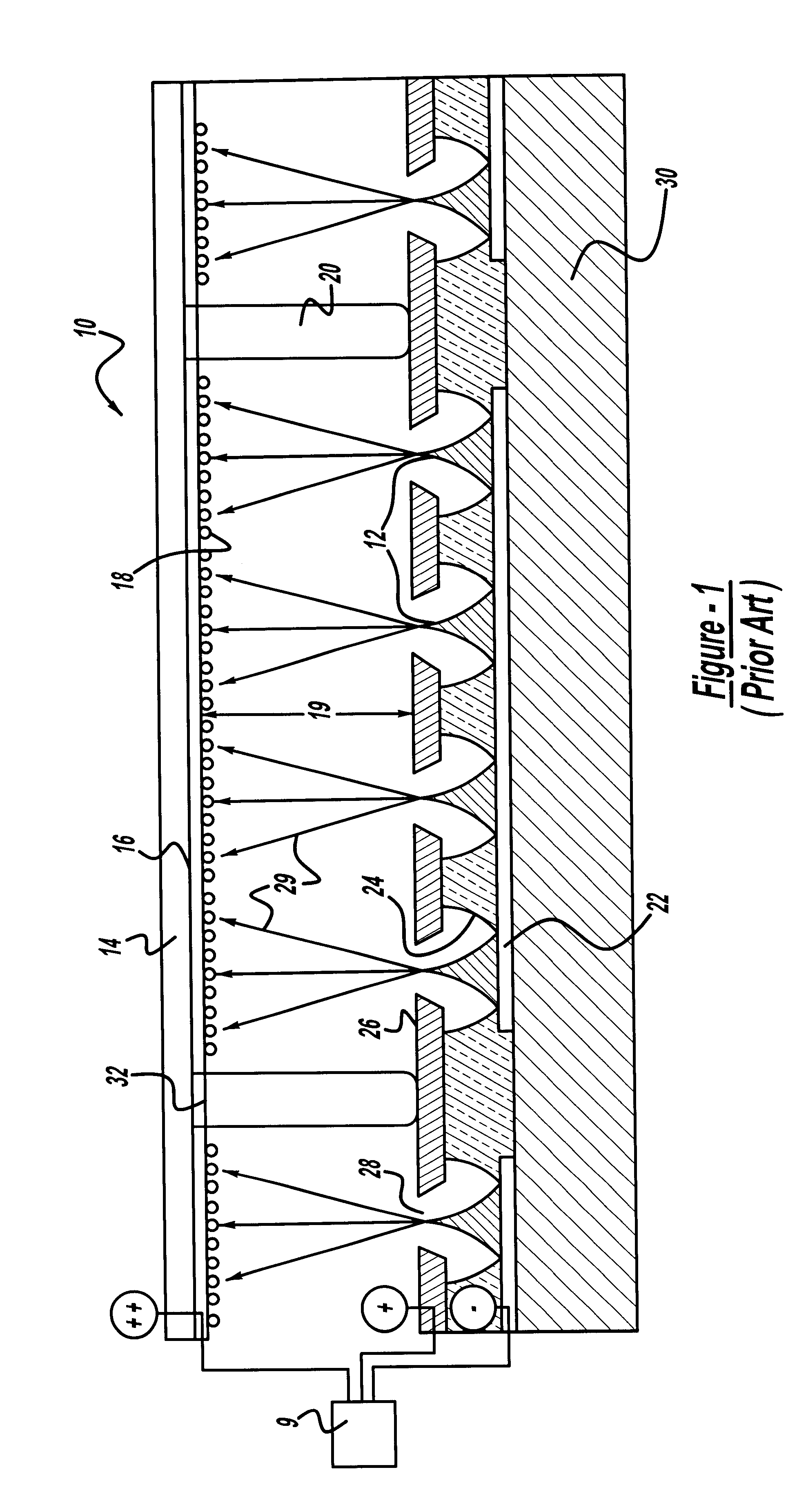
FIG. 1 schematically depicts an exemplary field emission display (FED) device 10 found within the prior art. This flat panel display comprises an x-y electrically addressable matrix of cold-cathode microtip or "Spindt" type field emitters 12 opposing a faceplate 14 coated with a transparent conductor layer 16 and a phosphor light emissive layer 18. A distance or gap 19, generally on the order of 100 to 200 .mu.m, is maintained between the emitters 12 and the phosphors 18 by spacers 20. The volume of space between the emitters 12 and the phosphors 18 is evacuated to provide a vacuum environment with a pressure generally in the range of 10.sup.-5 to 10.sup.-7 Torr. This environment is generally gettered (by means not illustrated) to mitigate against contamination of the internal parts, and to maintain the vacuum.

As illustrated, each emitter 12 has the shape of a cone and is coupled at its base to an addressable emitter electrode conductor strip or layer 22, through which the emitter 1...


PUM


Abstract

Cathodoluminescent field emission display devices features an electron amplification structure for generating secondary electron emissions. The electron amplification structure includes a channel structure having a bottom wall coupled to at least one side wall, thereby defining a channel cavity, and at least one protrusion extending from the side wall into the channel cavity. Furthermore, a primary electron source or emitter is provided for generating primary electron emission into the channel cavity, whereby secondary emissions of electrons are produced when the protrusion is bombarded by electrons within the channel structure. The use of a narrow channel in the electron amplification structure reduces the possibility that a returning ion will strike the emitter, and thus decreases cathode emitter tip erosion.

Description

This invention relates to electronic field emission display devices, such as matrix-addressed monochrome and full color flat panel displays in which light is produced by using cold-cathode electron field emissions to excite cathodoluminescent material. Such devices use electric fields to induce electron emissions, as opposed to elevated temperatures or thermionic cathodes as used in cathode ray tubes.Cathode ray tube (CRT) designs have been the predominant display technology, to date, for purposes such as home television and desktop computing applications. CRTs have drawbacks such as excessive bulk and weight, fragility, power and voltage requirements, electromagnetic emissions, the need for implosion and X-ray protection, analog device characteristics, and an unsupported vacuum envelope that limits screen size. However, for many applications, including the two just mentioned, CRTs have present advantages in terms of superior color resolution, contrast and brightness, wide viewing a...

Claims


Application Information

Patent Timeline
Patent Type & Authority Patents(United States)
IPC IPC(8): H01J29/06H01J31/12H01J3/02H01J29/02H01J29/46H01J29/08H01J1/304H01J3/00H01J1/30
CPCH01J1/304H01J3/022H01J29/06H01J29/085H01J29/467H01J29/482H01J31/127H01J2329/00H01J2329/46
Inventor JANNING, JOHN L.
Owner ST CLAIR INTPROP CONSULTANTS
Why Eureka
Try Eureka