
Solar cell, a method of producing the same and a semiconductor producing apparatus

a solar cell and production method technology, applied in the field of solar cells of high efficiency, a method of producing the same and an apparatus for producing a semiconductor, can solve the problems of preventing the formation of effective electrodes, utilizing a difference in etching rate at crystal planes, and not providing an antireflection

Inactive Publication Date: 2002-01-22
MITSUBISHI ELECTRIC CORP
View PDF12 Cites 60 Cited by
  • Summary
  • Abstract
  • Description
  • Claims
  • Application Information

AI Technical Summary

Problems solved by technology

However, this technique utilizes a difference of etching rate at crystal planes in a silicon crystal.
Thus steps which do not provide an antireflection effect and prohibits formation of effective electrodes are produced.
Further, the conventional method requires a long time for the treatment and is not high in productivity.
The conventional method of forming mechanically the V-like grooves requires grinding treatment for each wafer, and presents a problem in large scale production.
Further, the conventional technique requires a step of removing the defective layer by the wet type etching because there was a defect in the surface portion of crystal when the V-like grooves were formed.
However, the grooves cannot be formed with a small distance because the pitch of the V-like grooves is restricted by the pich of the rotating blades.
Accordingly, a crack may be produced in the substrate, or breakage may be caused during manufacturing steps when deep grooves are formed in the substrate.
However, there are problems such as a high manufacturing cost due to use of a vacuum device and a poor productivity due to a small performance of treatment.

Method used


Image

  • Solar cell, a method of producing the same and a semiconductor producing apparatus
  • Solar cell, a method of producing the same and a semiconductor producing apparatus
  • Solar cell, a method of producing the same and a semiconductor producing apparatus

Examples


embodiment 2

An example of a method of producing a solar cell in which a surface active agent is added (in about 580 ppm) into an etching liquid of mixed acid containing hydrofluoric acid, nitric acid and phosphoric acid as major components, will be described.

An etching liquid of mixed acid comprising a 50% hydrofluoric acid, a 69% nitric acid and a 85% phosphoric acid in the proportions of 12 parts by volume, 1 part by volume and 12 parts by volume is prepared, and an nonionic surface active agent of about 580 ppm is added thereto. A cast silicon substrate is dipped in the etching liquid of mixed acid for a time sufficient to obtain a predetermined etching quantity while the liquid is maintained at the room temperature. After the etching, the substrate is quickly taken out from the etching liquid and is transferred to a water tank filled with washing water in which washing is conducted by continuously supplying water to remove the etching liquid on the substrate. If a brown or black colored dep...

embodiment 3

An etching liquid of mixed acid comprising a 50% hydrofluoric acid, a 69% nitric acid and a 85% phosphoric acid in the proportions of 12 parts by volume, 1 part by volume and 12 parts by volume is prepared, and a nonionic surface active agent of about 580 ppm is added thereto. Further, ammonium fluoride of 30 g / l is added to the mixture. Then, a cast silicon substrate is dipped in the mixed etching liquid for a time to obtain a predetermined etching quantity while the liquid is kept at room temperature. After the etching, the substrate is quickly taken out from the liquid, and is transferred into a water tank filled with washing water in which washing is conducted by continuously supplying water to wash out the etching liquid on the substrate. However, if a brown or black-colored deposit remains on the substrate surface thus treated, the substrate is dipped in an aqueous solution of caustic soda or caustic potash having a concentration of several % to several ten % for several secon...

embodiment 4

An example of producing a solar cell by using a substrate wherein a minute projection / recess structure is formed in the surface according to the method described in Embodiment 2, will be explained.

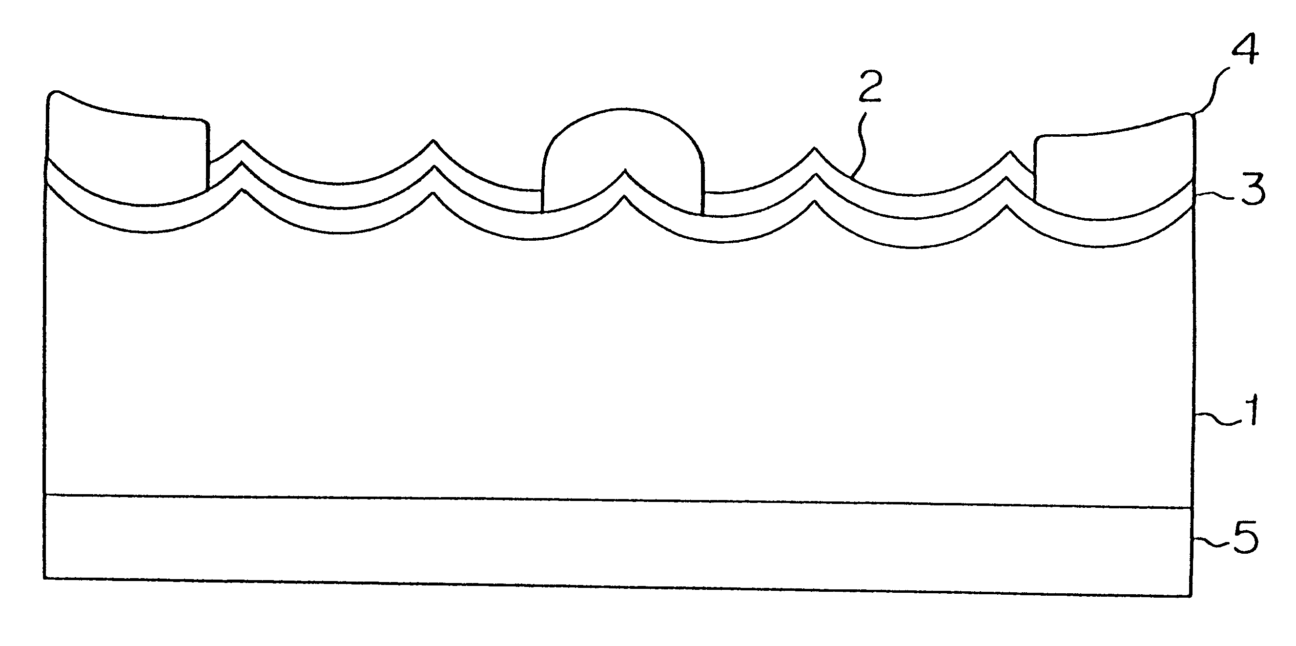
FIG. 8 is a cross-sectional view of an embodiment of the solar cell according to the present invention wherein numeral 1 designates a silicon substrate, numeral 2 designates an antireflection film formed on a plane to which light is incident, numeral 3 designates a n.sup.+ diffusion layer, numeral 4 designates a grid-like n electrode formed by sintering a silver paste, and numeral 5 designates a p electrode formed on a rear plane by sintering an aluminum paste or an aluminum-silver paste.

The p type polycrystal silicon substrate 1 in which a minute projection / recess structure was formed as described in Embodiment 2 was put in a diffusion furnace in which phosphorous oxychloride (POCl.sub.3) was used as a diffusion source, and phosphorous (P) was diffused by a vapor phase reaction to thereby...


PUM


Abstract

In preparing a solar cell, minute projections and recesses are uniformly formed in a surface of a single crystal silicon substrate or a polycrystal silicon substrate by dipping the substrate in an etching liquid of a mixed acid including a hydrofluoride acid, a nitric acid and an adjusting agent containing at least a phosphoric acid or a water-soluble carboxylic acid having a higher molecular weight than acetic acid for adjusting the etching rate of the etching liquid. A solar cell having a substrate in which spherical projections and recesses are formed in a surface thereof to which light is incident; an apparatus for producing a solar cell, and a wet etching apparatus to maintain a constant concentration of a nitric acid, are provided.

Description

1. Field of the InventionThe present invention relates to a solar cell of high efficiency, a method of producing the same and an apparatus for producing a semiconductor.2. Discussion of BackgroundIn order to obtain a silicon solar cell of high efficiency in its essential form minute projections and recesses in a substrate surface so that incident light entering from the substrate surface can be efficiently taken in the inside of the solar cell. Various methods have been proposed to realize such solar cell.In a solar cell of single crystal silicon, minute pyramidal projections and recesses called a texture structure are formed by a wet etching method by using an aqueous alkali solution such as caustic soda, caustic potash or the like. Because the texture structure is constituted by many inclined planes, light reflected at a surface hits a surface of another position and re-enters into the inside whereby the light is absorbed efficiently in the solar cell. A part of the incident light...

Claims


Application Information

Patent Timeline
Patent Type & Authority Patents(United States)
IPC IPC(8): H01L31/0236H01L31/18H01L21/306H01L31/04
CPCH01L31/0236H01L31/1804Y02E10/50H01L31/02363Y02E10/547Y02P70/50
Inventor NISHIMOTO, YOICHIROARIMOTO, SATOSHINAMBA, KEISUKE
Owner MITSUBISHI ELECTRIC CORP
Learn More