

Noncrystalline oxide semiconductor thin film, process for producing the noncrystalline oxide semiconductor thin film, process for producing thin-film transistor, field-effect-transistor, light emitting device, display device, and sputtering target
a technology of noncrystalline oxide and semiconductor, applied in the direction of metallic material coating process, solid-state device, diaphragm, etc., can solve the problems of difficult wet etching of oxide semiconductor itself, difficult to achieve large-scale and large-scale production, and difficult to pattern an electrode on an active layer, etc., to achieve easy to obtain large-area uniformity, improve the quality of large-size tft substrate, and increase the resistance to amorphous thin film
- Summary
- Abstract
- Description
- Claims
- Application Information
AI Technical Summary
Benefits of technology
Problems solved by technology
Method used
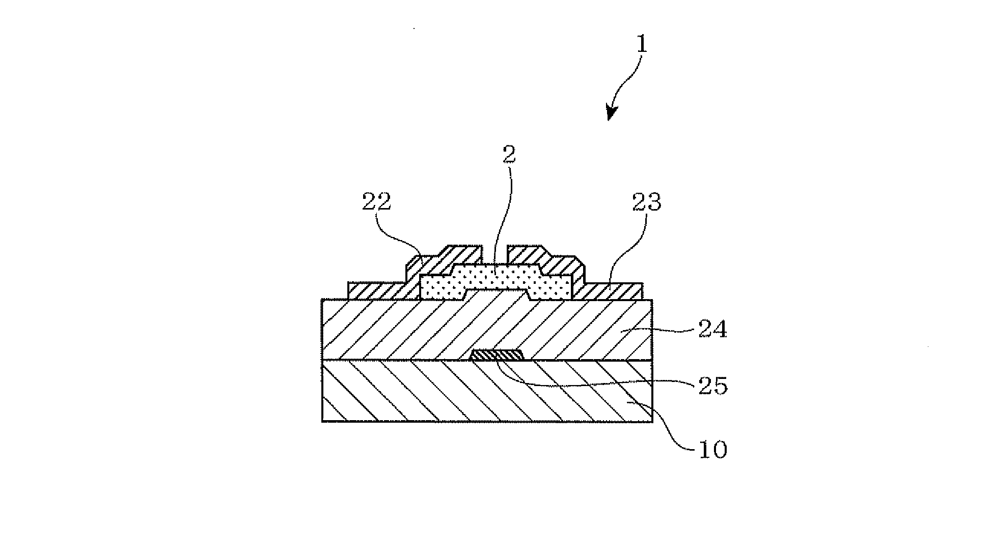
Image

Examples
example 1
(1) Production and Evaluation of Sputtering Target
1. Production of Target
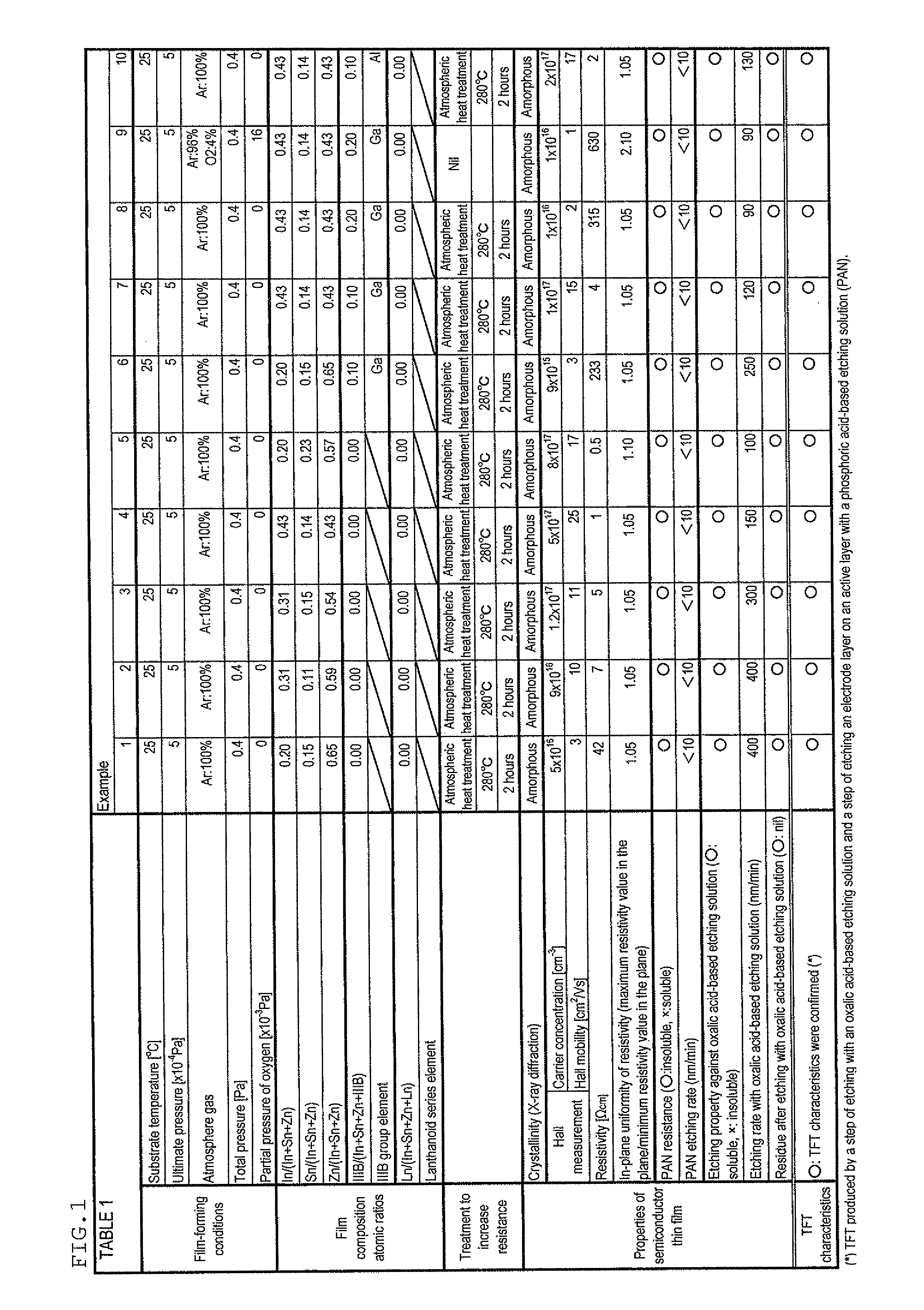
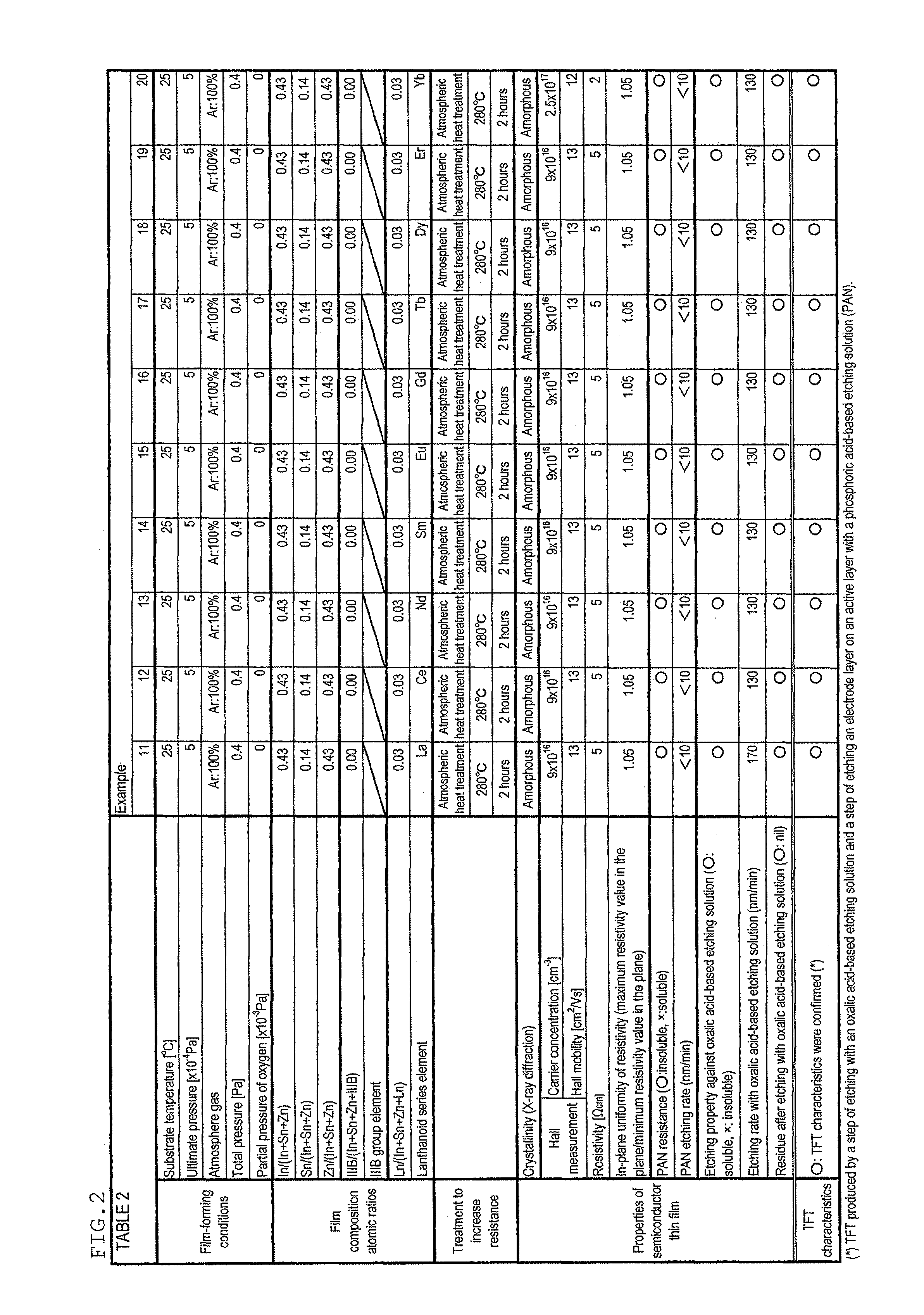
[0127]As the raw materials, indium oxide powder, tin oxide powder and zinc oxide powder were mixed such that [In] / ([In]+[Sn]+[Zn]) was 0.20, [Sn] / ([In]+[Sn]+[Zn]) was 0.15, and [Zn] / ([In]+[Sn]+[Zn]) was 0.65. The mixture was then supplied to a wet ball mill and mixed and pulverized for about 72 hours, whereby raw material fine powder was obtained.
[0128]After granulating the raw material fine powders, the raw material fine powder was press-molded to have a diameter of 10 cm and a thickness of 5 mm. The molded product was put in a firing furnace, and firing was performed at 1400° C. for 48 hours to obtain a sintered body (target). The heating rate was 3° C. / min.
2. Evaluation of Target
[0129]For the resulting target, the density and the bulk resistance were measured. As a result, it was found that the theoretical relative density was 98% and the bulk resistance value measured by the four probe method was 80 mΩ.
(2) ...
example 2
[0145]The amorphous oxide semiconductor thin film of Example 2 was produced in about the same manner as in Example 1 (film-forming conditions, film composition atomic ratios and treatment to increase resistance). The film composition was analyzed by the ICP method to find that the [In] / ([In]+[Sn]+[Zn]) was 0.31, the [Sn] / ([In]+[Sn]+[Zn]) was 0.11 and the [Zn] / ([In]+[Sn]+[Zn]) was 0.59.
[0146]The oxide semiconductor thin film produced under the above-mentioned production conditions has the properties as indicated in FIG. 1. It was found that the crystallinity was amorphous, the carrier concentration was 9×1016 cm−3, and the Hall mobility was 10 cm2 / Vs. The resistivity measured by the four probe method was 7 Ωcm. The in-plane uniformity of resistivity (maximum resistivity value in the plane / minimum resistivity value in the plane) was 1.05. The etching rate with the PAN etching solution was less than 10 nm / min, and the evaluation was good (insoluble). The etching rate with the oxalic ac...
example 3
[0147]The amorphous oxide semiconductor thin film of Example 3 was produced in about the same manner as in Example 1 (film-forming conditions, film composition atomic ratios and treatment to increase resistance). The film composition was analyzed by the ICP method to find that the [In] / [In]+[Sn]+[Zn]) was 0.31, the [Sn] / ([In]+[Sn]+[Zn]) was 0.15, and the [Zn] / [In]+[Sn]+[Zn]) was 0.54.
[0148]The oxide semiconductor thin film produced under the above-mentioned production conditions has the properties as indicated in FIG. 1. It was found that the crystallinity was amorphous, the carrier concentration was 1.2×1017 cm−3, and the Hall mobility was 11 cm2 / Vs. The resistivity measured by the four probe method was 5 Ωcm. The in-plane uniformity of resistivity (maximum resistivity value in the plane / minimum resistivity value in the plane) was 1.05. The etching rate with the PAN etching solution was less than 10 nm / min, and the evaluation was good (insoluble). The etching rate with the oxalic a...
PUM
| Property | Measurement | Unit |
|---|---|---|
| temperature | aaaaa | aaaaa |
| temperature | aaaaa | aaaaa |
| carrier density | aaaaa | aaaaa |
Abstract
Description
Claims
Application Information