Plasma generating apparatus and semiconductor manufacturing method
Inactive Publication Date: 2002-04-30
KOKUSA ELECTRIC CO LTD +1
View PDF4 Cites 33 Cited by
Summary
Abstract
Description
Claims
Application Information
AI Technical Summary
This helps you quickly interpret patents by identifying the three key elements:
Problems solved by technology
Method used
Benefits of technology
Benefits of technology
The gas introducer has the function of introducing the discharge gas and the reactive gas needed for plasma processing into the vacuum chamber. The exhaust has the function of exhausting the atmosphere present within the vacuum chamber to the outside, Since the vacuum chamber for processing the substrate is of rectangular configuration like the substrate, the vacuum chamber need not have excessively large volume in order to process a large-area rectangular substrate, thus improving the efficiency of utilization of the gas and the efficiency of utilization of the high-frequency discharge electrode. Since the discharge electrode for generating the plasma is also rectangular, the space in which the plasma is generated has the same rectangular shape as the substrate. Accordingly, the installation area required for the vacuum chamber can be reduced further, as a result reducing the area occupied thereby in the clean room in which it is installed and reducing the costs associated with clean room maintenance. Interaction between the high-frequency electrical field generated by supplying high-frequency power to the discharge electrode and the magnetic field created by the magnetic lines of force produced by the magnetic lines of force generator affords efficient gas discharge so that a high-density plasma may be formed within the plasma generating zone. With this arrangement, the efficiency of plasma generation may be improved by, for example, 10 times or more relative to ordinary capacitively coupled parallel plate systems.
Further, in the above mentioned semiconductor manufacturing method, it is preferable that the substrate is subjected to a predetermined plasma process while setting the internal pressure of said vacuum chamber within the range of from 0.1 Pa to 40 Pa. According to the semiconductor manufacturing method of the present invention, it is possible to produce a magnetron discharge through interaction of an electrical field and a magnetic field, which can be used for efficient plasma generation even at low gas pressures. Thus, high quality plasma processing of substrates is possible even at low pressures of from 0.1 Pa to 40 Pa within the vacuum chamber.
Problems solved by technology
This method requires relatively high temperatures, which may have a number of adverse effects on devices.
Since ordinary parallel plate high-frequency discharge plasma sources generate plasma rather inefficiently, the low film deposition rate poses problems when depositing a film on a substrate surface using plasma CVD.
Also, the uniformity of film thickness cannot be said to be adequate at present.
Using an ordinary parallel plate high-frequency discharge plasma source, when it is attempted to increase the high-frequency power input in order to increase the throughput of the apparatus, high sheath voltage tends to form on the cathode electrode surface to which the high frequency is applied, resulting in a serious problem of metalcontamination from the electrode surface.
Besides the parallel plate high-frequency discharge plasma sources, electron-cyclotronresonance (ECR) plasma sources, inductively-coupled plasma (ICP), micro surface wave, helicon wave, and other high-density plasma sources are also available, but while these give adequate plasma densities, they still have not reached plasma uniformity levels adequate for processing of large-area substrates.
The plasma generating apparatus disclosed in the above publication, however, has the drawback that high density plasma cannot be generated in the diametral central area of the plasma generation zone.
Accordingly, any plasma surface processing apparatus designed using this plasma generating apparatus will not be capable of surface processing under conditions of uniform plasma density.
Thus, with this design the rate of surface processing tends to be slow, and the efficiency of utilization of the gas and the efficiency of utilization of the electrodes tend to be poor.
Where the magnetic field at the substrate surface is too strong to be ignored (20 gauss or above, for example), an uneven plasma distribution will be produced at the substrate surface, making uniform processing impossible.
The magnetic field also causes charges to build up on the substrate surface, which may damage the substrate.
Method used
Image
Click on the blue label to locate the original text in one second.
Reading with bidirectional positioning of images and text.
Examples
embodiment 1
[1] Embodiment 1
[1-1] Design
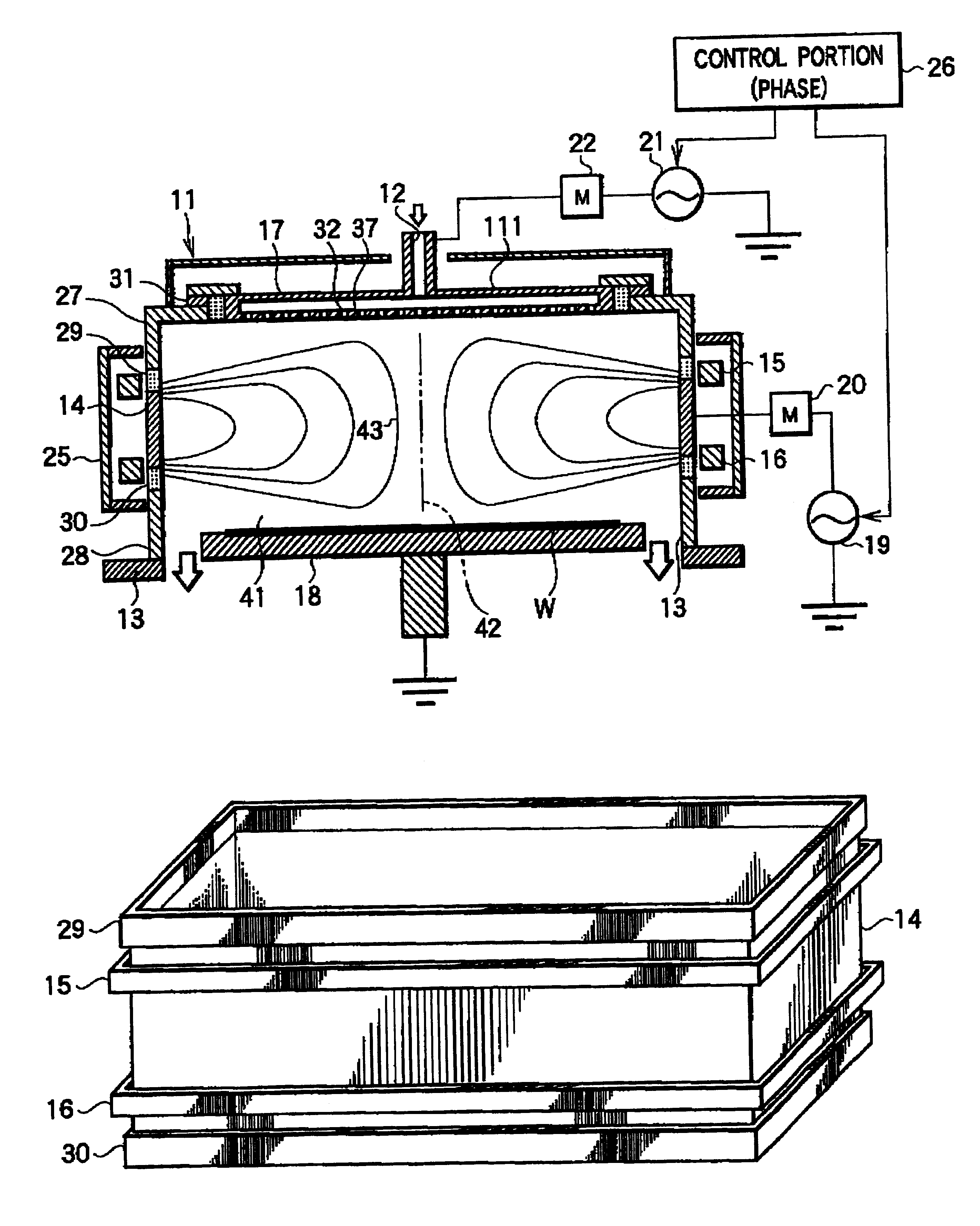
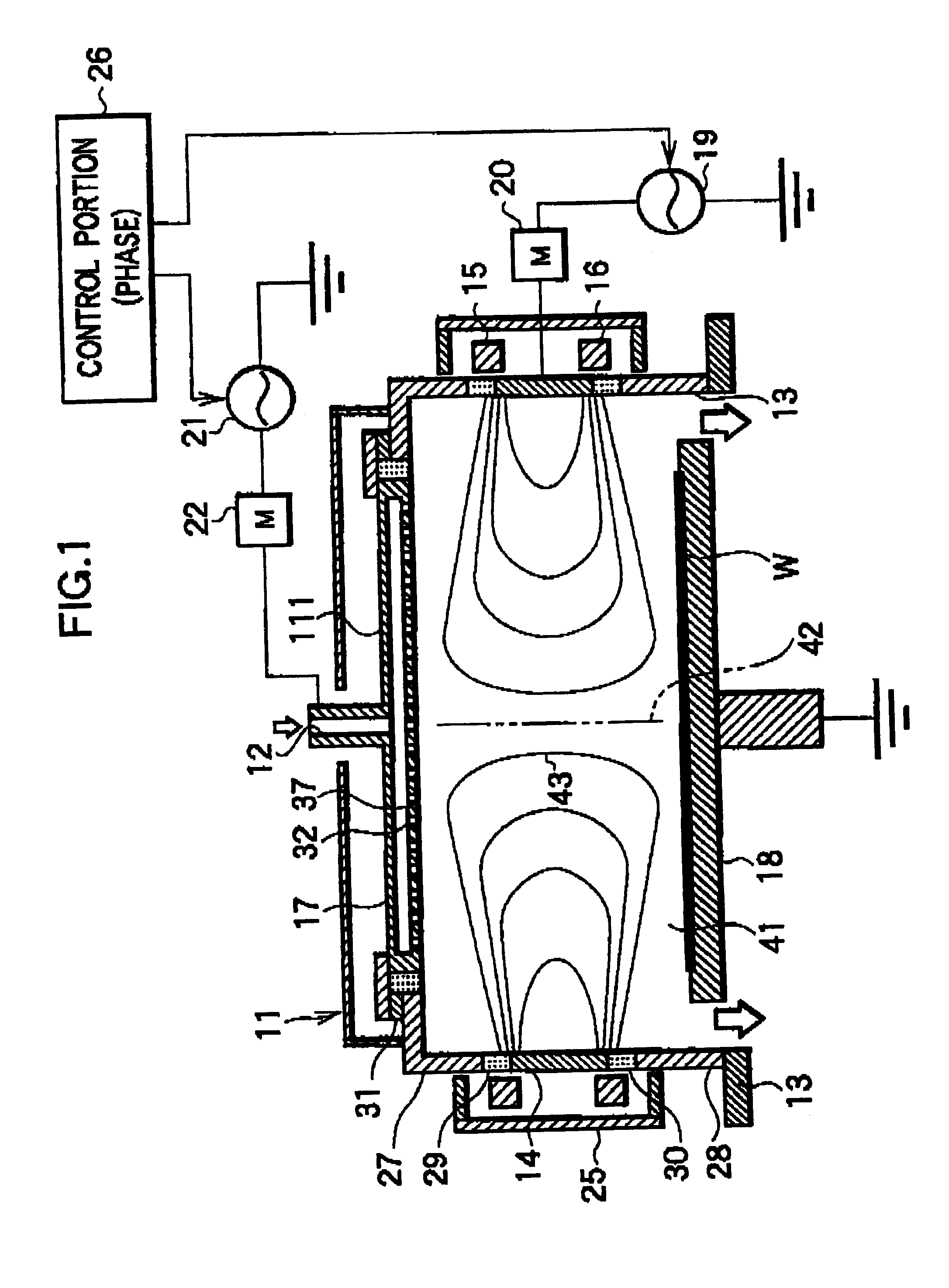
FIG. 1 is a side sectional view of the design of a first embodiment of the invention.
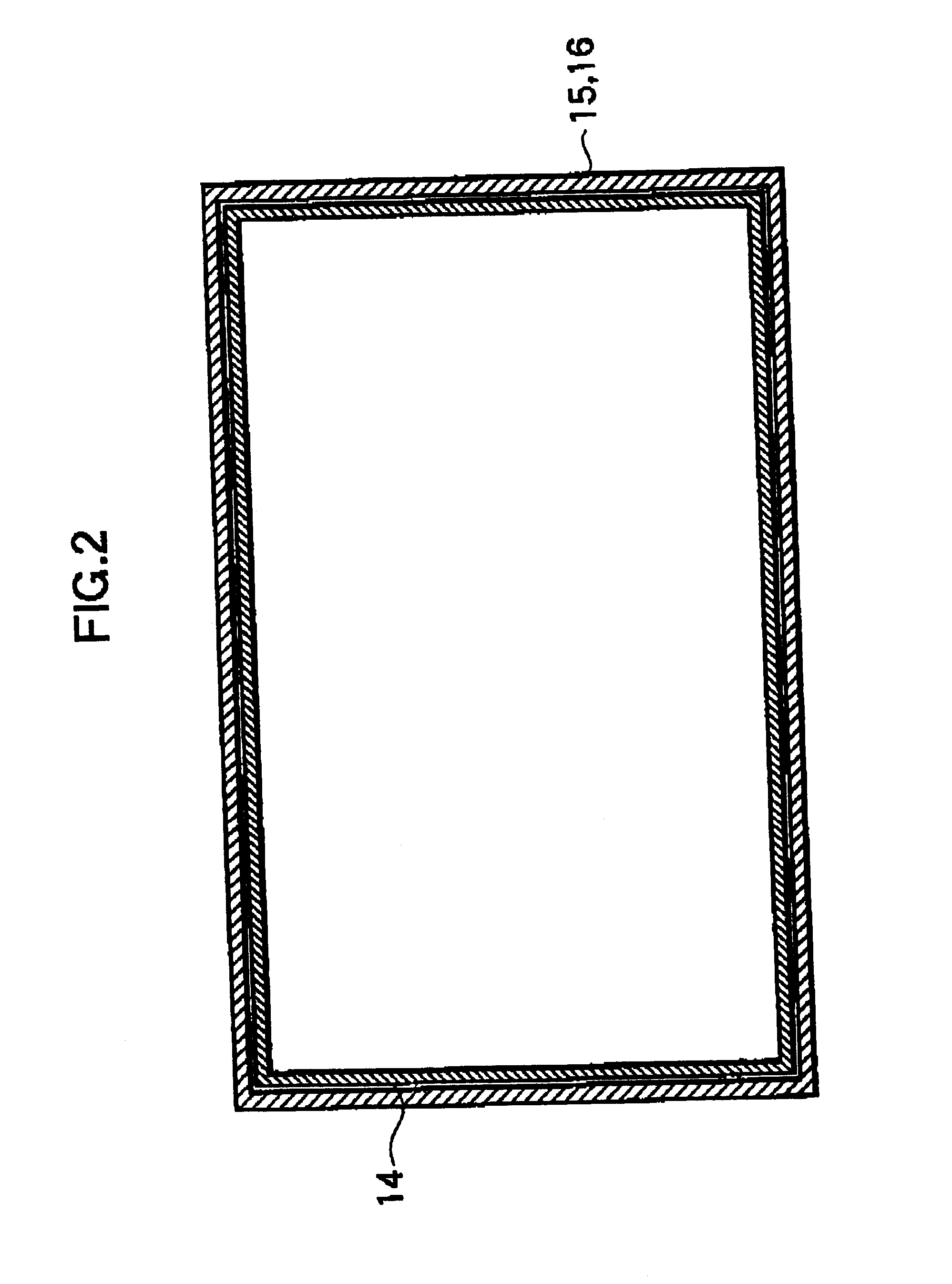
The plasma generating apparatus of the present embodiment comprises a vacuum chamber 11, a gas introduction portion 12, an exhaust portion 13, a discharge electrode 14, a pair of permanent magnets 15, 16, a pair of parallel plate electrodes 17, 18, a first high-frequency generator 19, a first matching circuit 20, a second high-frequency generator 21, a second matching circuit 22, a high-frequency shielding cover 25, and a control portion 26.
Vacuum chamber 11 is an airtight chamber provided therein with a plasma generating zone 41, and is of rectangular fistulous form such that when cut across the horizontal, the resulting aperture is rectangular, at least on the inside perimeter thereof. Here, the entire cross section, including the exterior perimeter, is rectangular. Vacuum chamber 11 is arranged in such a way that a center axis thereof is oriented vertically, for exampl...
embodiment 2
[2] Embodiment 2
FIG. 5 is a simplified illustration of a design according to a second embodiment of the invention. While fundamentally identical to the apparatus shown in FIG. 1, to this simplified illustration dispenses with the details in order to emphasize the differences therefrom. This treatment shall be adopted the third and subsequent embodiments, described later, as well.
In the preceding first embodiment, high-frequency power is applied to top electrode 17. In the present embodiment, however, high-frequency power from the second high-frequency oscillator 21 is applied to bottom electrode 18, with top electrode 17 being grounded. This design affords substantially the same working effect as the preceding embodiment, but provides the following additional advantages.
According to the present embodiment, top electrode 17 is grounded, whereby the sheath voltage on the surface of top electrode 17 can be held to a low level. As a result, damage to top electrode 17 by sheath voltage c...
embodiment 3
[3] Embodiment 3
FIG. 6 is a simplified illustration of a design according to a third embodiment of the invention. In the preceding second embodiment, top electrode 17 is grounded. In the present embodiment, however, top electrode 17 is electrically floating. This design affords even lower sheath voltage on the surface of top electrode 17 than does the Embodiment 2. Further reductions in damage to top electrode 17 by sheath voltage and in sheath voltage-induced metalcontamination of top electrode 17 are afforded thereby.
PUM
Property
Measurement
Unit
Force
aaaaa
aaaaa
Pressure
aaaaa
aaaaa
Polarity
aaaaa
aaaaa
Abstract
A plasma generating apparatus and processing method, which generate high-density plasma, even in the central portion of the plasma generating zone. The apparatus comprises rectangular electrodes, a rectangular fistulous dischargeelectrode which surrounds the plasma generating zone, and a vacuum chamber of rectangular cross-section. Permanent magnets surround the dischargeelectrode, produce predetermined magnetic lines of force with portions which extend approximately parallel to the central axis of dischargeelectrode. A pair of parallel plate electrodes define the extension of the plasma generating zone in the direction of the central axis of the discharge electrode. The apparatus is configured such that the magnetic lines of force passing through the central portion of the plasma generating zone do not intersect with the electrodes.
Description
1. Field of the InventionThe present invention relates to a modified magnetron high-frequency discharge plasma generating apparatus and to a semiconductor manufacturing method, and more particularly to an apparatus for performing various processes on rectangular substrates using a plasma, such as plasma dry etching of a film formed on the surface of a large-area rectangular substrate, or suitable as a plasma CVD (chemical vapor deposition) apparatus for producing a thin film on the surface of a substrate using a plasma-induced vapor phase reaction.2. Description of the Related ArtIn production processes for solid state devices such as semiconductor devices, it is necessary to subject substrates to predetermined processes. One such substrate processing method involves introducing a reactive gas into the reaction chamber in which the process will be performed, and applying heat to induce the gas to react so as to deposit a film on the substrate surface. This method requires relatively...
Claims
Application Information
Patent Timeline
Application Date:The date an application was filed.
Publication Date:The date a patent or application was officially published.
First Publication Date:The earliest publication date of a patent with the same application number.
Issue Date:Publication date of the patent grant document.
PCT Entry Date:The Entry date of PCT National Phase.
Estimated Expiry Date:The statutory expiry date of a patent right according to the Patent Law, and it is the longest term of protection that the patent right can achieve without the termination of the patent right due to other reasons(Term extension factor has been taken into account ).
Invalid Date:Actual expiry date is based on effective date or publication date of legal transaction data of invalid patent.

