Method for manufacturing photoelectric conversion device

Inactive Publication Date: 2002-05-07
SHARP KK
View PDF11 Cites 48 Cited by
  • Summary
  • Abstract
  • Description
  • Claims
  • Application Information

AI Technical Summary

Benefits of technology

When the plasma process is performed each time the second p-layer reached the predetermined thickness, at least one of the frequency, irradiation time and power is preferably decreased sequentially. Such a plasma process makes it possible to gradually increase the light absorption coefficient of the second p-layer as it is closer to the i-layer, i.e., to gradually suppress increase of the amount of light absorbed in the first p-layer. As a result, the short-circuit current can be improved, and reduction of Voc and F. F. can be suppressed. For example, the above-described conditions for the plasma process may be set as shown in Table 1.
The second p-layer may be formed with the same film forming apparatus as that used for the formation of the first p-layer, e.g., in the same chamber as that of a plasma CVD apparatus. In this case, the p-type impurities existing in the atmosphere used for the formation of the first p-layer may be introduced without designing any special doping profile. Consequently, there is formed the second p-layer with a certain doping profile which decreases the light absorption coefficient. That is, increase in the am

Problems solved by technology

However, when plasma of B.sub.2 H.sub.6 gas is generated on such a metal oxide film, boron radicals abstract hydrogen which terminates bonds of Si in the a-Si film and a great number of uncombined bonds referred to as "dangling bonds" are formed, causing reduction of the metal oxide film.
This increases the amount of light absorption of the p-layer serves as a window layer and decreases the light transmittance of the metal oxide film, which results in a remarkable decrease in a short-circuit current of the device.
In addition, since boron in the plasma also increases uncombined bonds on the surface of the film, a great number of recombination levels are generated at the p-i interface, which significantly causes a harmful influence on conversion efficiency.
For example, when a SiC film doped with boron is used as the p-layer, the film is not preferably bonded to the photoelectric conversion layer, which makes it impossible to maintain sufficient Voc and F.F. Accordingly, a buffer layer (intrinsic SiC film) is normally inserted at the p-i interface.
However, this layer is less conductive, which increases the internal resistance of the device and consequently reduces F.F.
Thus, delicate adjustments must

Method used


Image

  • Method for manufacturing photoelectric conversion device
  • Method for manufacturing photoelectric conversion device
  • Method for manufacturing photoelectric conversion device

Examples


embodiment 2

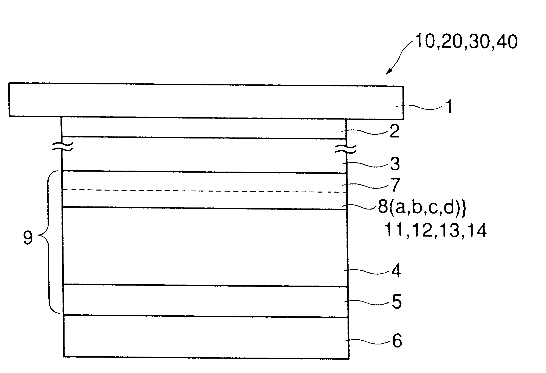
In the present embodiment, as shown I FIG. 1, a tandem photoelectric conversion device 20 is provided by forming a transparent electrode layer 2, a first pin junction layer 3, a p-layer 12, an i-layer 4 and an n-layer 5 that comprises a second pin junction layer 9 and a back electrode layer 6 in the order listed on a transparent glass substrate 1. In this example, the p-layer 12 is formed of a first p-layer 7 and a second p-layer 8b, and the second p-layer 8b is formed by a method of manufacture in which a plasma process is performed on the surface of the second p-layer 8b every time it is deposited to a predetermined thickness.

A method for manufacturing the tandem photoelectric conversion device 20 will be described below.

First, an uneven transparent glass substrate 1 with a transparent electrode layer 2 made of ZnO was placed on a substrate supporting body in a p-layer forming chamber of a plasma gas phase film forming apparatus, and a pin junction layer 3 constituted of an a-Si l...

embodiment 3

In the present embodiment, as shown I FIG. 1, a tandem photoelectric conversion device 30 is provided by forming a transparent electrode layer 2, a first pin junction layer 3, a p-layer 13, an i-layer 4 and an n-layer 5 that comprise a second pin junction layer 9 and a back electrode layer 6 in the order listed on a transparent glass substrate 1. In this example, the p-layer 13 is formed of a first p-layer 7 and a second p-layer 8c. The second p-layer 8c is formed by a method of manufacture in which a plasma process is performed on the surface of the second p-layer 8c for a plasma irradiation time and / or with reduced processing power each time the second p-layer 8c of a predetermined thickness is obtained.

A method for manufacturing the tandem photoelectric conversion device 30 will be described below.

First, an uneven transparent glass substrate 1 with a transparent electrode layer 2 made of ZnO was placed on a substrate supporting body in a p-layer forming chamber of a plasma gas ph...

embodiment 4

In the present embodiment, as shown I FIG. 1, a tandem photoelectric conversion device 40 is provided by forming a transparent electrode layer 2, a first pin junction layer 3, a p-layer 14, an i-layer 4 and an n-layer 5 that comprise a second pin junction layer 9 and a back electrode layer 6 in the order listed on a transparent glass substrate 1. In this example, the player 14 is formed of a first p-layer 7 and a second p-layer 8d. The second p-layer 8d is formed by a method of manufacture in which a plasma process is performed on the surface of the first p-layer 7 after the first p-layer 7 is formed.

A method for manufacturing the tandem photoelectric conversion device 40 will be described below.

First, an uneven transparent glass substrate 1 with a transparent electrode layer 2 made of ZnO was placed on a substrate supporting body in a p-layer forming chamber of a plasma gas phase film forming apparatus, and a pin junction layer 3 made of a-Si was fabricated on the substrate 1. A ma...


PUM


Abstract

A photoelectric conversion device including a plurality of pin junction layers, wherein at least a p-layer adjacent to an n-layer is formed of a stack of an amorphous silicon layer as a first p-layer and an amorphous silicon layer as a second p-layer, the first p-layer having a thickness of 5 nm or less and containing a p-type impurity and an n-type impurity, and the second p-layer having a p-type impurity concentration gradually decreasing as it is closer to an i-layer.

Description

This application is related to Japanese application No. Hei 11(1999)-150270 filed on May 28, 1999 and Hei 11(1999)-374085 filed on Dec. 28, 1999, whose priorities are claimed under 35 USC .sctn.119, the disclosure of which are incorporated by reference in those entirety.1. Field of the InventionThe present invention relates to a photoelectric conversion device and a method for manufacturing the same. More particularly, it relates to a photoelectric conversion device to be used for a thin film solar battery or the like formed by sandwiching a pin junction layer as a photoelectric conversion layer with electrodes, and a method for manufacturing the same.2. Description of the Related ArtVarious efforts have been made on the development of doped layers provided on the light-incident side of thin film solar batteries, which are one of important factors that relate to improvement of conversion efficiency. Especially, various researches are being made on p-layers which are one of doped lay...

Claims


Application Information

Patent Timeline
IPC IPC(8): H01L21/02H01L21/20H01L31/06H01L31/075H01L31/20H01L31/18H01L31/076
CPCH01L31/076H01L31/202Y02E10/548Y02P70/50
Inventor KISHIMOTO, KATSUSHI
Owner SHARP KK
Why Eureka
Try Eureka