
Semiconductor device with power cutting transistors

a technology of power cutting transistor and semiconductor device, which is applied in the direction of power consumption reduction, pulse technique, instruments, etc., can solve the problems of insufficient transistor cut-off, inability to accept the speed of operation to decrease, and too large sub-threshold current to be ignored

Inactive Publication Date: 2002-07-02
RENESAS ELECTRONICS CORP
View PDF2 Cites 17 Cited by
  • Summary
  • Abstract
  • Description
  • Claims
  • Application Information

AI Technical Summary

Problems solved by technology

Thus, it is not acceptable for the speed of operations to decrease in order to accomplish low voltage operation.
However, when the threshold voltage is reduced to enable high speed operation of the transistor, the transistor can no longer cut-off sufficiently.
In the case of products typified by a low-power consuming SRAM in which there are many transistors and the standby current is very small, this sub-threshold current is too large to be ignored.
However, if the threshold voltage of the transistor is raised in order to reduce the leak current, then a longer delay results, and an improvement in speed cannot be anticipated.
However, since these are all high Vt transistors, the subthreshold current is small.
For this reason, the electric potential output from the semiconductor device becomes unstable.
However, the circuit design in the semiconductor device of Conventional Example 3 becomes complicated in this case, and the chip size is increased as a result.
As a result, the sub-threshold current that is problematic in the standby state does not flow to these transistors.
However, the semiconductor device of this conventional example 4 has the following problems.

Method used


Image

  • Semiconductor device with power cutting transistors
  • Semiconductor device with power cutting transistors
  • Semiconductor device with power cutting transistors

Examples


first embodiments

[First Embodiments]

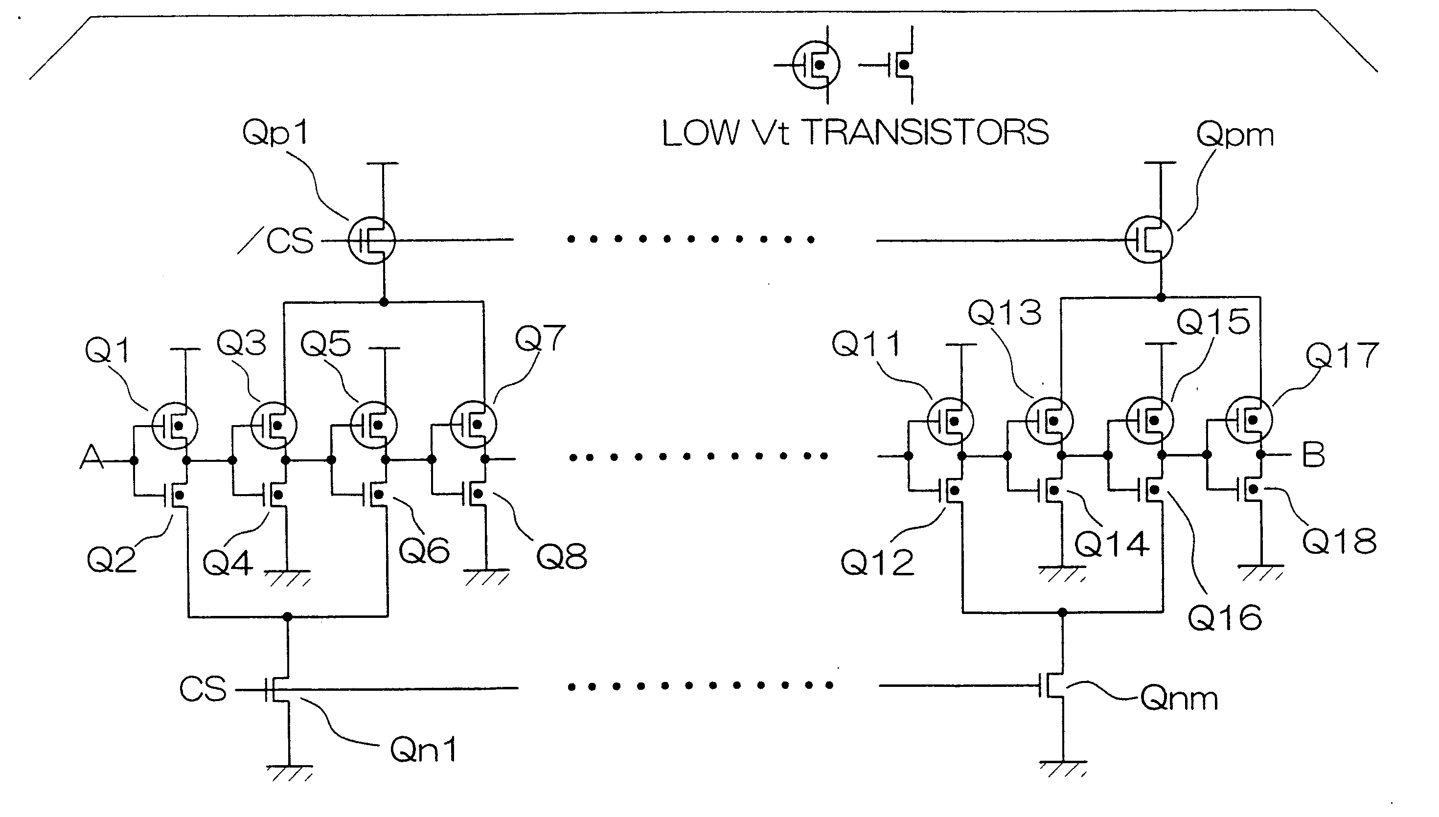
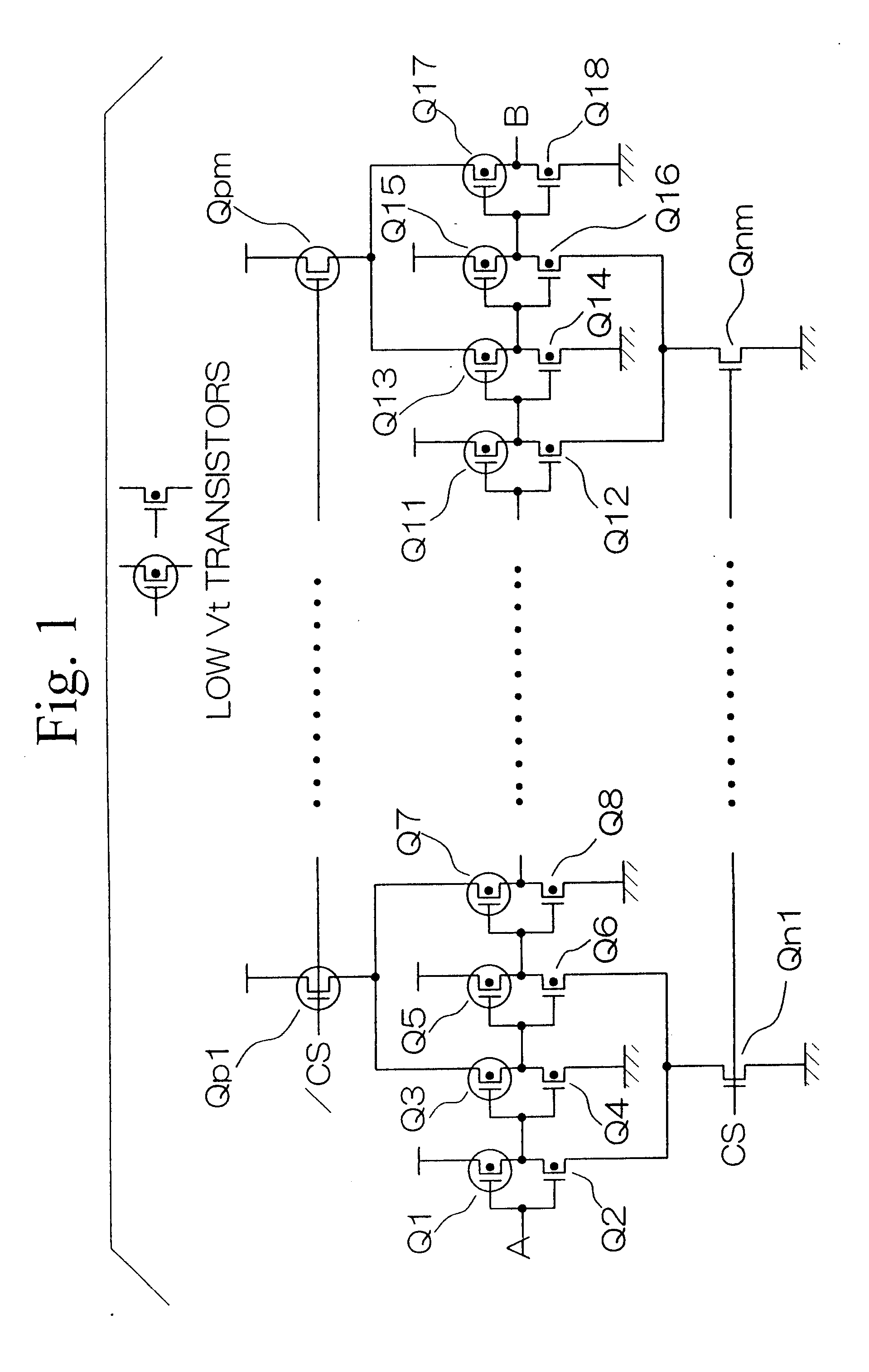
FIG. 1 is a circuit diagram showing the structure of a semiconductor device according to the present embodiment. The circuit in FIG. 1 is a logic circuit in which multiple stages of inverters are dependently connected. TrQ1.about.TrQ8 and TrQ11 .about.TrQ18 in the figure are all low Vt transistors, and form a logic circuit extending from input node A to output node B. TrQn1.about.TrQnm and TrQp1.about.TrQpm (where m is a natural number which is 2 or greater) are all high Vt power cutting transistors which have a threshold voltage that is set to be higher than the aforementioned low Vt transistors. Note that this figure shows only the first four stages of inverters after node A and the last four stages of inverters before output node B. This embodiment considers that the electric potential of input node A when the semiconductor device is in a standby state is at "L" level.

In this embodiment, the propagation delay time per stage of inverters is 1 ns each, for exampl...

second embodiment

[Second Embodiment]

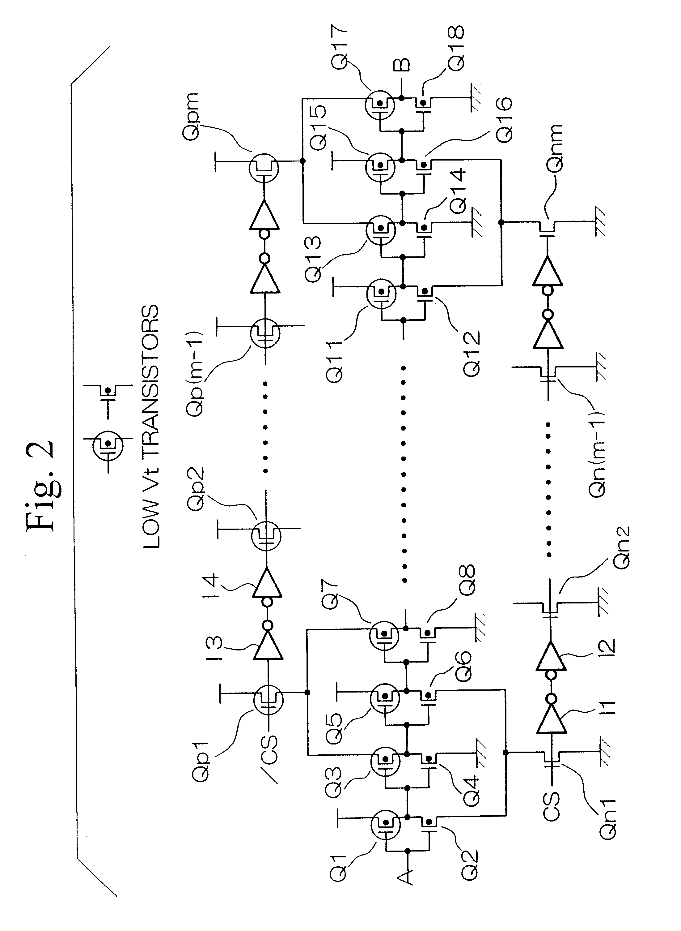
FIG. 2 is a circuit diagram showing the structure of a semiconductor device according to the present embodiment. Structural elements that are the same as those shown in FIG. 1 have been assigned the same numerical symbol. In the first embodiment, chip selecting signal CS was supplied to all of the gate terminals of power cutting transistors TrQn1.about.TrQnm, and chip selecting signal / CS was supplied to all of the gate terminals of power cutting transistors TrQp1.about.TrQpm. In other words, in the first embodiment, all of the power cutting transistors are driven by drivers (omitted from the figures) that are provided respectively to chip selecting signals CS, / CS.

In contrast, in this embodiment, respective buffers have been added in between the gate terminals of the power cutting transistors that were connected in common in the first embodiment. For example, a buffer, in which inverters I1 and I2 are dependently connected, is inserted in between the gate termina...

third embodiment

[Third Embodiment]

FIG. 3 is block diagram showing the overall structure of a semiconductor device according to the present invention, and shows an example of the design of the SRAM to which the present invention is applied. In this figure, memory cell array 1 is of the typical form in which memory cells are disposed at the points of intersection between word lines which are in rows and bit lines which are in columns. Address ADD is an access address that is supplied from outside the SRAM, and includes the row address and column address.

Address buffer 2 buffers the row address that is included in address ADD and outputs the result as row address RA. Address buffer 3 buffers the column address that is included in address ADD and outputs the result as column address CA. In addition, address buffer 2 detects transformations in the row address at each bit, and outputs this detected result as an address transformation detection signal ATDC. Similarly, address buffer 3 detects transformati...


PUM


Abstract

A semiconductor device that operates at high speed using a low voltage power source, in which the output of each gate in the standby state is stable, and which has a delay time that is not affected by the frequency of the input signal.TrQ1 to TrQ8, which form multiple stages of the inverters are designed to have a low threshold voltage in order to accomplish low voltage operation. When input node A is at "L" in the standby state, TrQ2, Q3, Q6, and Q8 which cut-off are connected to high threshold voltage TrQn1 and Qp1. In the standby state, power cutting TrQn1 and Qp1 cut off in accordance with chip selecting signals CS, / CS, thereby blocking the flow of sub-threshold current to TrQ1~Q8. Since TrQ1, Q4, Q5 and Q8 are not cut off at this time, the output potential of each inverter is stable. The number of transistors assigned to each power cutting transistor is determined based on the frequency of the input signal, so that only one transistor from among the transistors connected to TrQn1 and Qp1 will be ON at any given time.

Description

1. Field of the InventionThe present invention relates to a semiconductor device that has a low current consumption and performs high-speed operations using a low-voltage electrical source. More specifically, the present invention relates to a semiconductor device that is suitable for use in SRAM (static random access memory) and similar devices having a small standby current.2. Description of the Related ArtIn recent years, LSI (large-scale integrated circuits) and other such logic circuits have tended to operate using a low-voltage power source. The reason for this trend is that the withstanding voltage declines as the size of the transistors (abbreviated as "Tr" hereinafter) for forming logic circuits is reduced. Accordingly, the operating voltage must be reduced as a necessity. In addition, in order to install LSIs in portable information devices, it is essential for these LSI to be capable of being operated by the battery devices and therefore, these LSIs must be operated at lo...

Claims


Application Information

Patent Timeline
Patent Type & Authority Patents(United States)
IPC IPC(8): G11C11/418G11C11/419G11C11/417H03K19/00G11C11/413G11C11/41G11C11/412H03K19/0948
CPCG11C11/417G11C11/418G11C11/419H03K19/0016G11C11/412
Inventor MIZUGUCHI, ICHIRO
Owner RENESAS ELECTRONICS CORP
Learn More