Process and structure for 50+ gigahertz transistor

Inactive Publication Date: 2002-07-02
GLOBALFOUNDRIES INC
View PDF7 Cites 36 Cited by
  • Summary
  • Abstract
  • Description
  • Claims
  • Application Information

AI Technical Summary

Problems solved by technology

It is known that many limitations on frequency of operation derive from parasitic capacitances and resistances which have been reduced only at substantial cost and which appear to have reached a point of diminishing returns.
Other efforts to increase operational frequency or bandwidth of transistors have largely concentrated on exotic materials and device complexity; both tending to increase transistor cost and the latter tending to reduce manufacturing yield due to the intricacy and/or criticality of transistor structures and correspondingly complex processes by which they are formed.
Further gains in operating frequency and bandwidth are complicated by a requirement for manufacturing compatibility with other types of transistors such as complementary metal-oxide-semiconductor (CMOS) field effect transistors in integrated circuits used as support signal pro

Method used


Image

  • Process and structure for 50+ gigahertz transistor
  • Process and structure for 50+ gigahertz transistor
  • Process and structure for 50+ gigahertz transistor

Examples


Example

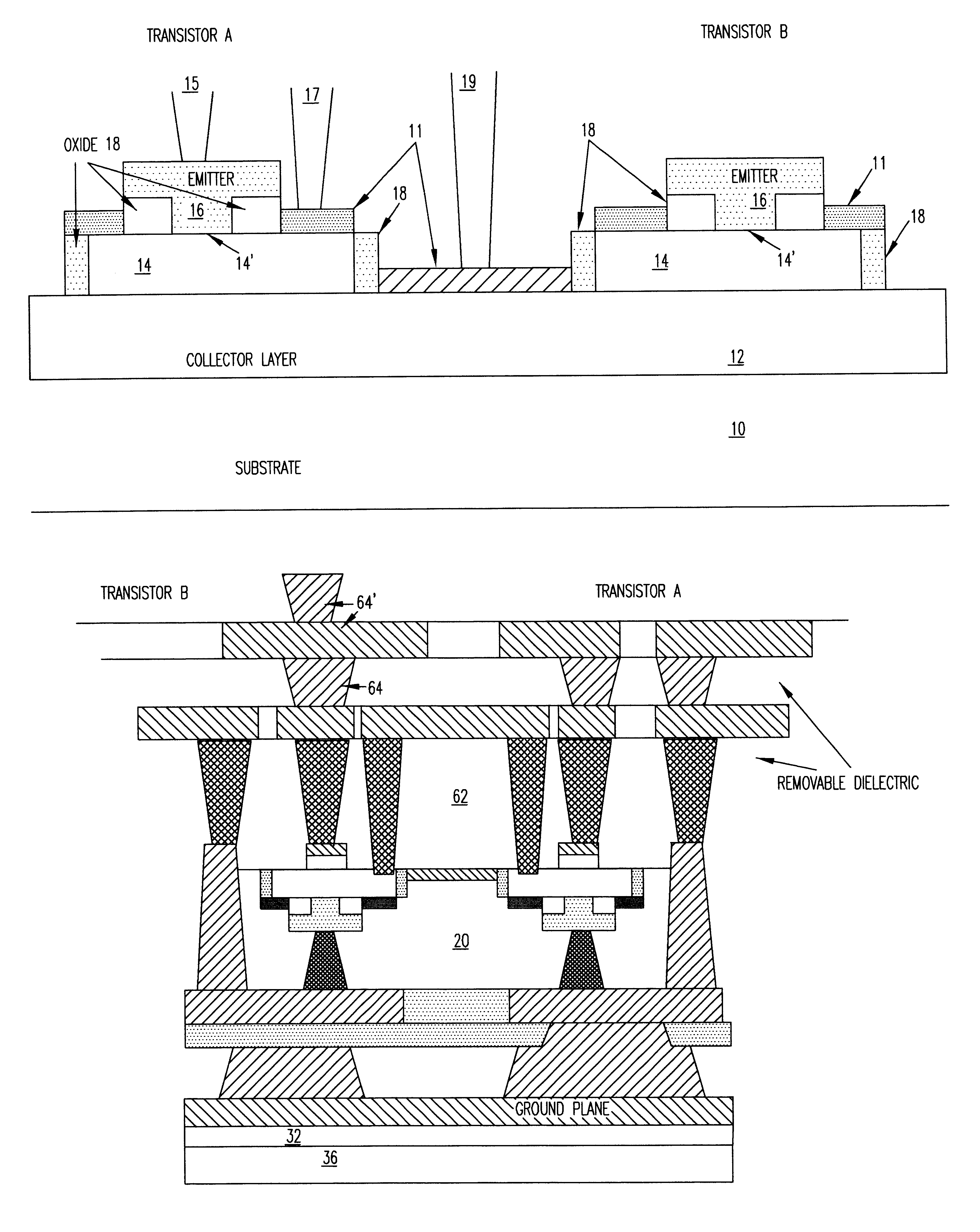
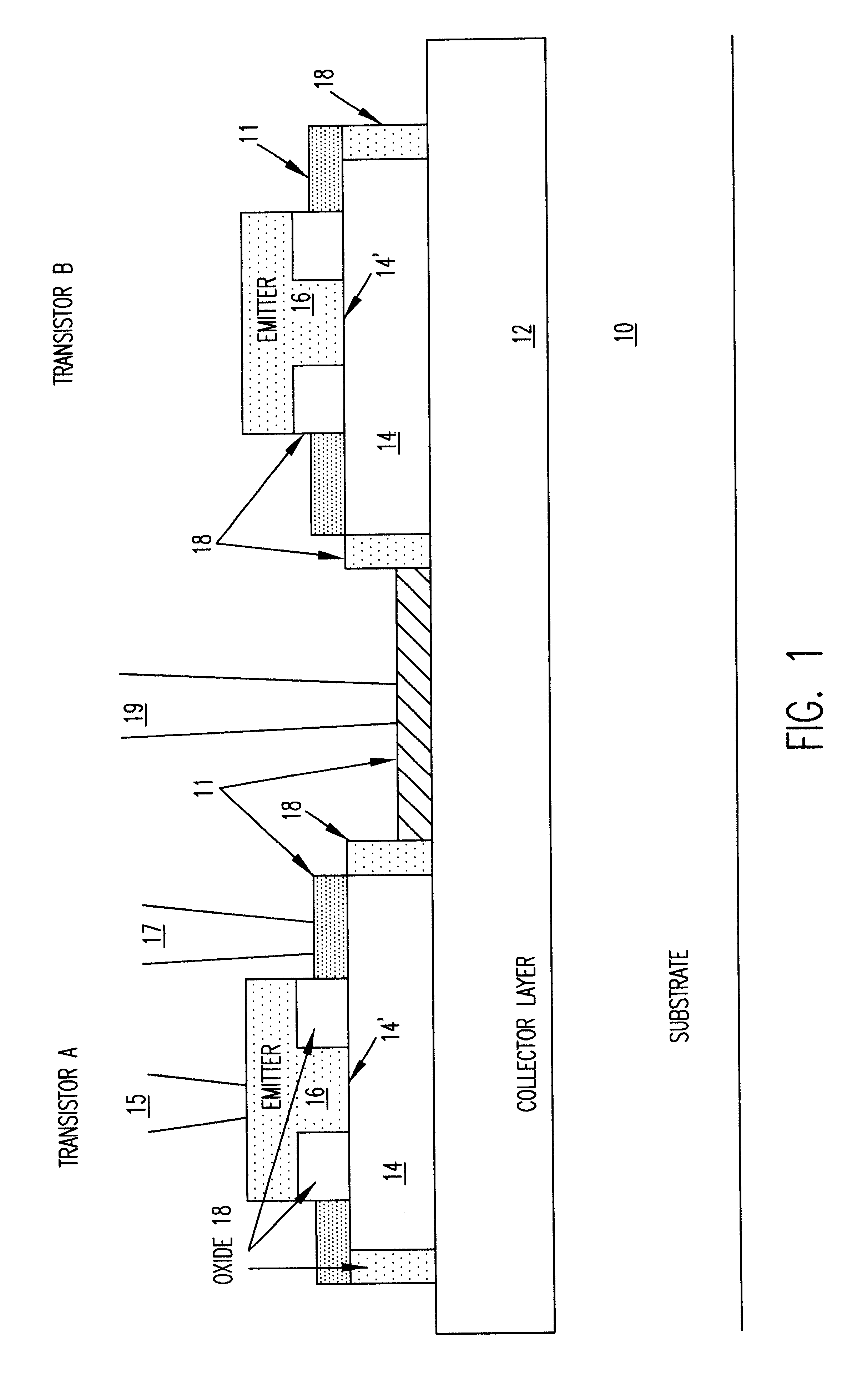
Referring now to the drawings, and more particularly to FIG. 1, there is shown, in cross-sectional view, two exemplary transistors of arbitrary design formed on a single substrate. The illustration of two transistors is intended to demonstrate that the invention is applicable to integrated circuit devices and to provide illustration of how some exemplary, generally desirable, features of the application of bipolar transistors to integrated circuits are accommodated and provided for some transistors to the exclusion of other transistors. Since the particulars of the transistor design depicted is intended to be arbitrary (and is substantially unimportant to the practice of the invention), no portion of FIG. 1 is admitted to be prior art as to the present invention, even though the invention is applicable to well-known transistor designs and the design depicted may resemble other known transistor structures.

The invention represents a substantial departure from current trends in develop...


PUM


Abstract

High frequency performance of transistor designs is enhanced and manufacturing yield improved by removing and reducing sources of parasitic capacitance through combinations of processes from different technologies. After formation of collector, base and emitter regions on a substrate and attachment of a second substrate, the original substrate is wholly or partially removed, the inactive collector area is removed or rendered semi-insulating and wiring and contacts are made from the original back side of the chip. Dielectric material used in the manufacturing process can be removed to further reduce capacitance. The high frequency transistors can be bonded to CMOS chips or wafers to form BICMOS chips.

Description

1. Field of the InventionThe present invention generally relates to high performance transistors operable to microwave frequencies and, more particularly, to high performance transistor designs compatible with MOS / CMOS field effect transistors in integrated circuit designs.2. Description of the Prior ArtThe increase in amount of information transferred or distributed electronically has generated a substantial demand for increased bandwidth of data processing arrangements and high frequency communication links. Computer clock frequencies in excess of 1 Gigahertz (GHz) have been projected within a relatively few years. Microwave frequencies up to 50 GHz are currently in use. High speed data links are currently operating at 40 Gigahertz and frequencies of 100 Gigahertz are foreseeable. Additionally, high frequency communication links provide some substantial advantages in that the radiation pattern from a relatively small antenna can be readily constrained to limit required transmissio...

Claims


Application Information

Patent Timeline
IPC IPC(8): H01L21/02H01L21/70H01L21/8222H01L21/331H01L27/082H01L21/768H01L29/73H01L21/8248H01L21/8249H01L27/06
CPCH01L21/8222H01L27/0823H01L29/66242
Inventor FREEMAN, GREGORY G.GROVES, ROBERT A.JOHNSON, JEFFREYSUBBANNA, SESHADRIVOLANT, RICHARD P.
Owner GLOBALFOUNDRIES INC
Why Eureka
Try Eureka