Integrated hybrid optoelectronic devices

a hybrid optoelectronic and integrated technology, applied in the direction of instruments, semiconductor lasers, photomechanical apparatuses, etc., can solve the problems of inability to detect polarization, low loss devices, and the effect of wdm on the affecting of nearly all optical network systems

Inactive Publication Date: 2002-08-20
THE ARIZONA BOARD OF REGENTS ON BEHALF OF THE UNIV OF ARIZONA
View PDF16 Cites 42 Cited by
  • Summary
  • Abstract
  • Description
  • Claims
  • Application Information

AI Technical Summary

Problems solved by technology

In customer optoelectronic systems, large bandwidth, polarization insensitive, low loss devices are required for multi-channel broadcasting.
Furthermore, wavelength division multiplexing (WDM) soon will impact nearly all optical network systems.
Due to the diverse characteristics of each of these components, integration onto a singular substrate is an imposing problem with conventional fabrication procedures and standard optical glass materials.
Here, as with WDM, integration of optical components onto a singular substrate represents a complex problem.
However, one obstacle for application of sol-gel inorganic materials into optical devices is the limitation imposed by the maximum attainable crack-free sol-gel glass thickness.
Thus, these processes are costly and time consuming.
However, these materials were require rigorous synthesis and patterning procedures, not conducive to optical device integration.
Thus, a number of issues regarding loss inherent from the sol-gel processing have not been resolved which limit the application of sol-gel processing and thus restrict optical device integration, especially between diverse active and passive optical components.
These issues include inherent losses in the sol gel glasses at the operating frequency, unintentional losses due to light scatter at sol-gel glass / air interfaces, and improper design of passive optical components.
As a consequence of the complexities of the integration process and the lack of a suitable sol-gel medium, optoelectronic systems coupling light output from photoelectronic devices into power splitters and beam steering elements have not been integrated onto a singular substrate.

Method used


Image

  • Integrated hybrid optoelectronic devices
  • Integrated hybrid optoelectronic devices
  • Integrated hybrid optoelectronic devices

Examples


Embodiment Construction

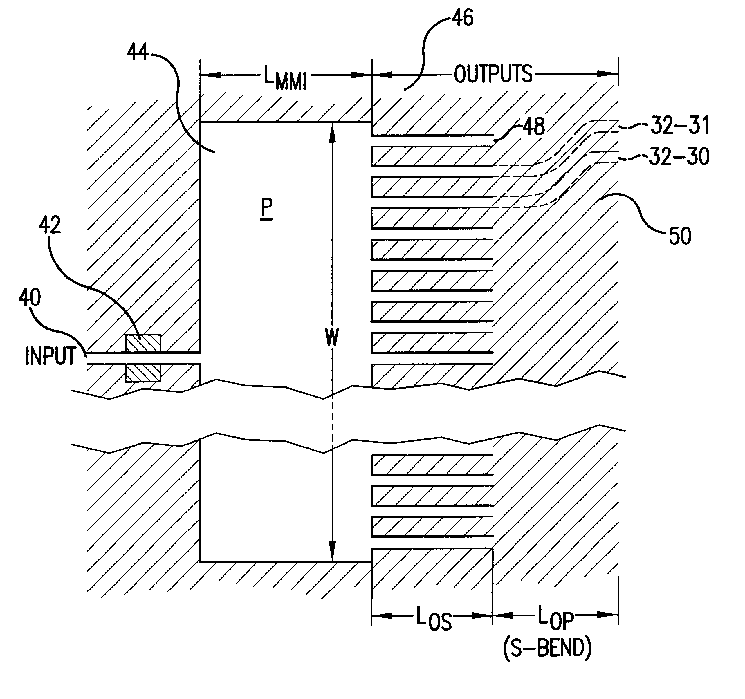
Referring now to the drawings, wherein like reference numerals designate like or corresponding parts throughout the several views, and more particularly to FIG. 1a thereof, FIG. 1a is a flow chart showing processing steps according to the present invention which based on sol gel processing produce hybrid optoelectronic devices integrating passive optical components with active optoelectronic components. Fabrication of hybrid optoelectronic devices using sol-gel processing requires, in addition to lossless sol gel materials, a detailed knowledge of the optical properties of the cured sol gel material, such as optical loss, optical index, optical index dispersion, and polarization sensitivity. The fabrication process utilizes steps which integrate the sol-gel materials with traditional optical materials and active optoelectronic components such that unintentional losses from light scattering are avoided. Control of these losses depends not only on the internal and surface properties o...


PUM

PropertyMeasurementUnit
mole %aaaaaaaaaa
thicknessaaaaaaaaaa
temperaturesaaaaaaaaaa

Abstract

A hybrid optoelectronic device and method of producing the hybrid device in which the hybrid device includes a substrate with an input region configured to accept input light, a sol-gel glass multimode interference region coupled to and contiguous with the input region and configured to accept and replicate the input light as multiple self-images, and a sol-gel glass output region contiguous with the multimode region and configured to accept and to output the multiple self-images. Alternatively, the hybrid optoelectronic device includes a substrate with a photoelectronic device, a surface resonator including a light-emitting part of the photelectronic device and configured to resonate light from the photoelectronic device to produce a laser light, and a grating outcoupler contiguous with the surface resonator and configured to diffract the laser light outward from the grating outcoupler and to electrically vary an index of refraction of the outcoupler and change a direction of the diffracted laser light.

Description

1. Field of the InventionThe present invention relates to production of hybrid optoelectronic devices which integrate active optoelectronic and passive optical components into novel hybrid optical devices to be used in optoelectronic systems.2. Discussion of the BackgroundIn customer optoelectronic systems, large bandwidth, polarization insensitive, low loss devices are required for multi-channel broadcasting. Optical component processing based on self-imaging devices such as multimode interference (MMI) devices is an attractive choice for fabrication. Indeed, due to excellent optical properties and ease of fabrication, multimode interference (MMI) devices have already found applications in laser modulators, splitters, switches, and receivers. Production MMI power splinters, as compared with conventional 1.times.2 waveguide branches, yield devices with smaller dimensions and do not suffer from non-uniformity of output power as a result of sharp edges near the waveguide branches.From...

Claims


Application Information

Patent Timeline
Patent Type & Authority Patents(United States)
IPC IPC(8): G02B6/132G02B6/13G02B6/28G02B6/12G02B6/122G02B6/138G03F7/00H01S5/026H01S5/00H01S5/20
CPCG02B6/12004G02B6/122G02B6/132G02B6/138G02B6/2813G03F7/0005G02B2006/12107G02B2006/12121G02B2006/12173H01S5/026H01S5/2081
Inventor FALLAHI, MAHMOUDFARDAD, AMIR
Owner THE ARIZONA BOARD OF REGENTS ON BEHALF OF THE UNIV OF ARIZONA
Why Eureka
Try Eureka