

Methods and apparatus for generating spatially resolved voltage contrast maps of semiconductor test structures
a voltage contrast map and spatial resolution technology, applied in semiconductor/solid-state device testing/measurement, semiconductor/solid-state device details, instruments, etc., can solve the problems of increasing the time required to scan voltage contrast data to perform comparisons, adding more complexity to circuits, and requiring such small dimensions. , to achieve the effect of easy drying, improved and timely information, and convenient processing
- Summary
- Abstract
- Description
- Claims
- Application Information
AI Technical Summary
Benefits of technology
Problems solved by technology
Method used
Image

Examples
Embodiment Construction
)
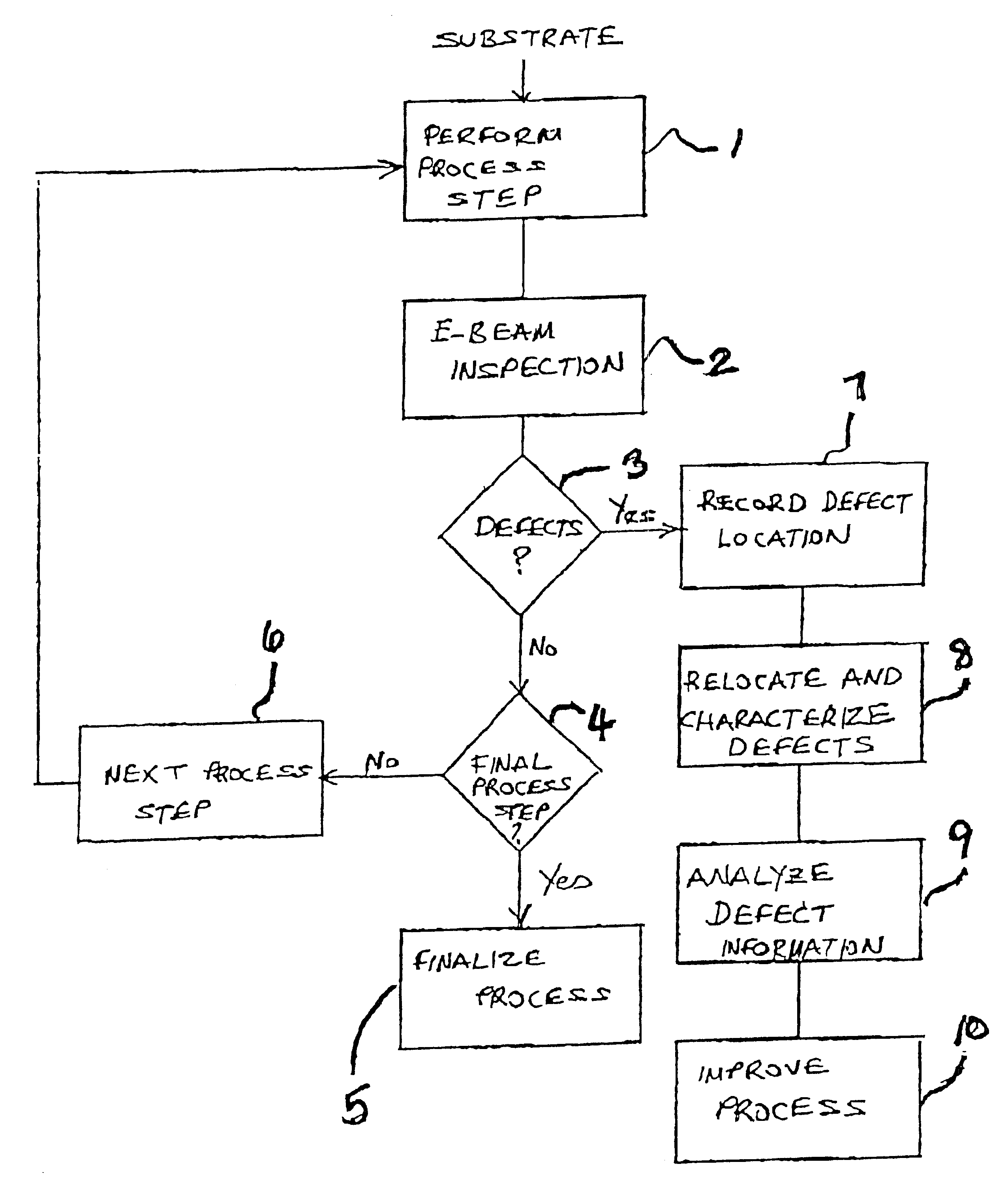
As will be further described below, the preferred embodiment of the present invention provides automated, rapid, contactless wafer inspection capabilities in order to detect, isolate and characterize electrical defects impacting integrated circuits.
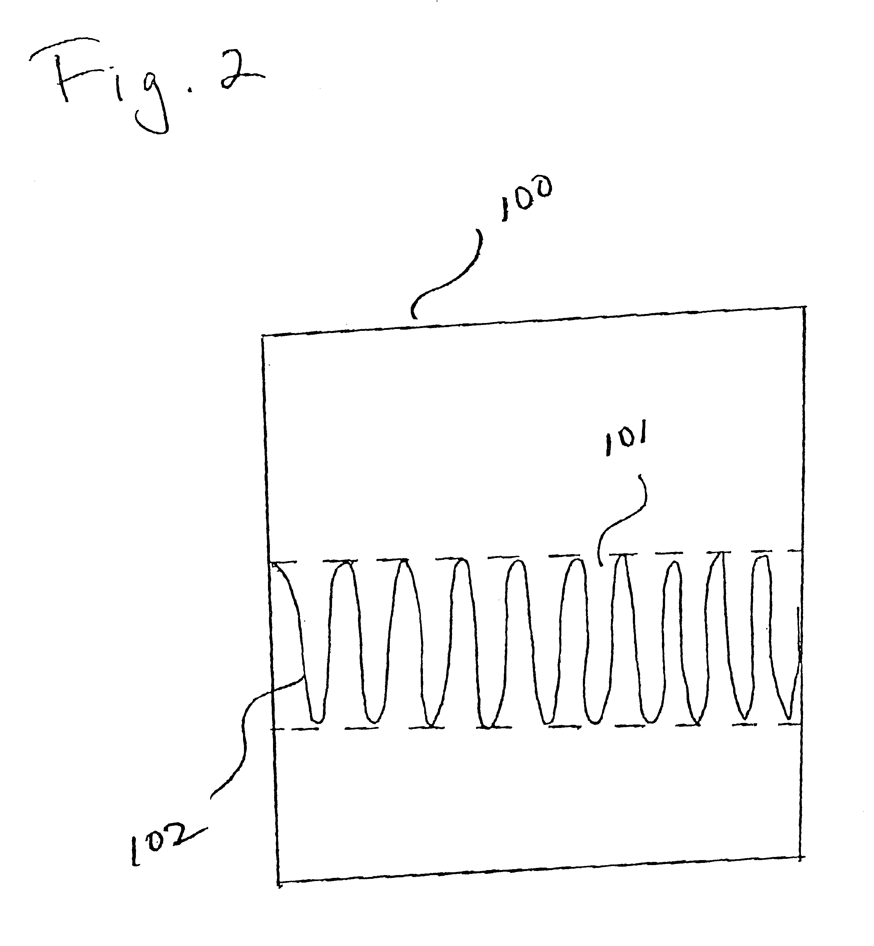
Several embodiments of the present invention are described herein in the context of exemplary multilevel integrated circuit structures, including semiconductor structures and overlying metallization or other interconnects, using various levels of conductors that are separated from each other and the substrate by dielectric layers. However, structures formed using other methods of semiconductor fabrication also fall within the scope of the present invention.
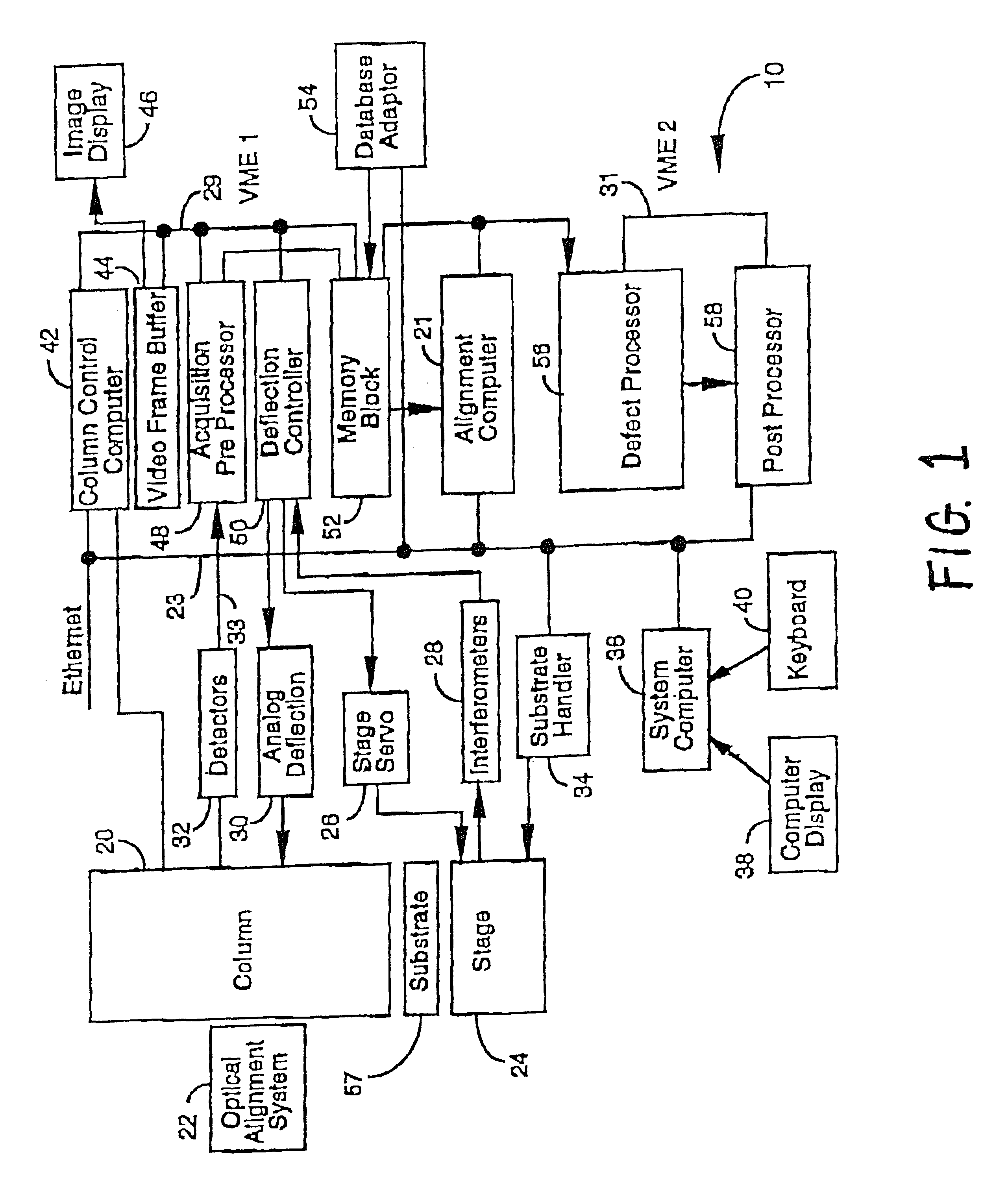
One application of the present invention includes the operation of a scanning electron microscope (SEM) with a continuously moving stage. However, the test structures and many of the methods described herein are also useful in the context of other testing devices, including SEM's opera...
PUM
| Property | Measurement | Unit |
|---|---|---|
| pixel resolution sizes | aaaaa | aaaaa |
| speeds | aaaaa | aaaaa |
| width | aaaaa | aaaaa |
Abstract
Description
Claims
Application Information