Thin film transistor and semiconductor device and method for forming the same

a thin film transistor and semiconductor technology, applied in the direction of transistors, semiconductor devices, electrical appliances, etc., can solve the problems of high cost, insufficient polycrystal silicon thin film transistors to meet the scale-up and speed-up needs of devices, and inability to obtain stable and uniform characteristics

Inactive Publication Date: 2002-11-12
SEMICON ENERGY LAB CO LTD
View PDF11 Cites 14 Cited by
  • Summary
  • Abstract
  • Description
  • Claims
  • Application Information

AI Technical Summary

Problems solved by technology

This is not a critical problem, for example when it is used to perform a switching operation of each pixel of a liquid crystal display or each bit of an image sensor, but is a critical problem particularly in a switching speed when a drive circuit is constructed on same substrate.
However, the polycrystal silicon thin film transistor is also insufficient to satisfy scale-up and speed-up needs of a device.
In addition, in most cases, cost is high because of use of expensive quartz as a substrate.
However, the thin film transistor grown in solid phase on the quartz substrate by above method has not only a problem that stable and uniform characteristics cannot be obtained because of lack of uniformity of thermal contraction of quartz, but also a problem that there occurs a failure due to an instability phenomenon that reduction of off resistance and current-curve variation with time lapse are developed, and these problems make it difficult to realize large-area device.
In addition, the quartz substrate is more expensive several times than glass, especially for a large-area substrate, so that the quartz would be unsuitable as substrate in this respect.
In addition, since the thermal contraction of the substrate exceeds 200 ppm in a heating process for activating impurities doped in the thin film transistor, a pattern alignment is difficult even using a reduction projecting light exposure device having a mechanism of correcting a substrate expansion and contraction, especially when the diagonal length of the substrate exceeds 10 inches.
Further, there is a problem in the thin film transistor forming process that if the substrate is contracted in a process after the patterning treatment, an alignment process cannot be carried out in a next process.

Method used


Image

  • Thin film transistor and semiconductor device and method for forming the same
  • Thin film transistor and semiconductor device and method for forming the same
  • Thin film transistor and semiconductor device and method for forming the same

Examples


Embodiment Construction

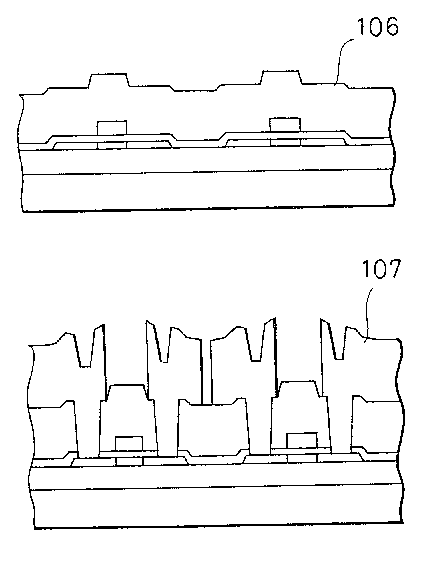
An example using a low alkali glass different from that of the embodiment 1 will be shown as a comparison example. First, a pre-anneal process was carried out at 600.degree. C. for 48 hours, and a solid-phase growth was carried out by the annealing treatment at 600.degree. C. for 48 hours. The subsequent processes were identical to those of the embodiment 1. In this process, the thermal contraction were measured to be 900 to 1000 ppm in the solid-phase growth process and 300 ppm in the activation process.

It was found from the measurement of the characteristics of the thin film transistor thus obtained that a threshold voltage is shifted to a positive gate voltage side by 3 to 4 volts for NMOS and by 2 to 3 volts for PMOS as shown in FIGS. 4(a) and (b). In addition, a phenomena that rise-up of a current value of the PMOS is sluggish was observed.

Further, in the processes, the mask alignment was very difficult because the thermal contraction of the substrate in the activation treatmen...


PUM

PropertyMeasurementUnit
threshold voltageaaaaaaaaaa
thicknessaaaaaaaaaa
temperatureaaaaaaaaaa

Abstract

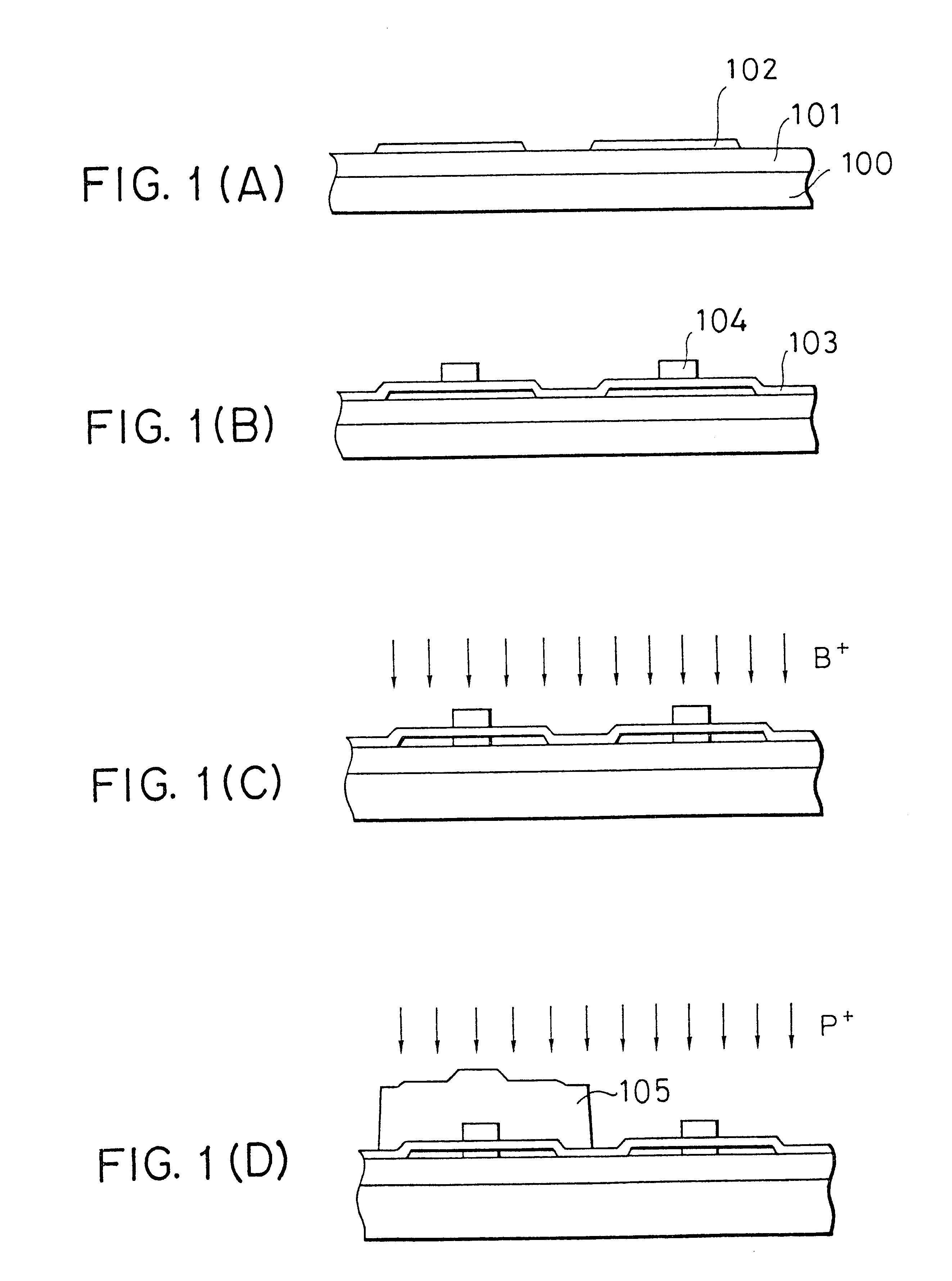
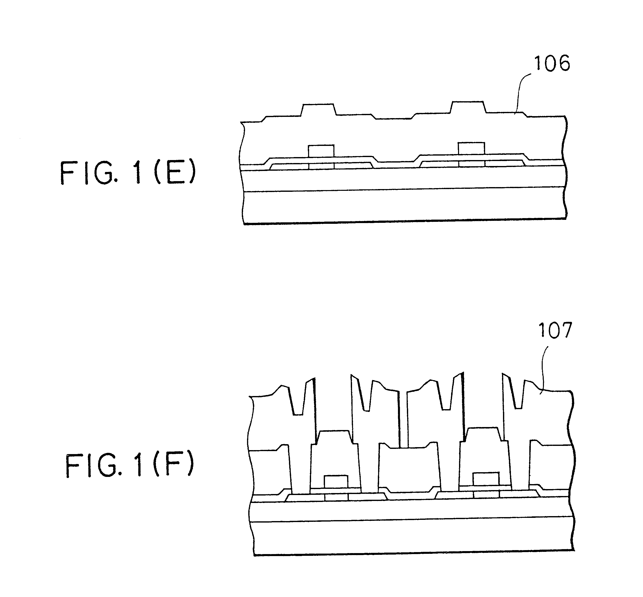
A thin film transistor and a semiconductor device and a method for forming the same. A silicon thin film formed on an insulating substrate is heated at 550 to 800° C. so that it has crystallinity, and a thin film transistor is formed using the crystalline silicon film thus obtained. Thermal contraction of the insulating substrate is set in a range of 30 to 500 ppm in the heating process, so that the thin film transistor has high mobility, low threshold voltage and high off-resistance. Thermal contraction of the insulating substrate may be also set 100 ppm or less in a heating process after a patterning treatment in a thin film transistor producing process.

Description

1. Field of the InventionThis invention relates to a thin film transistor and a semiconductor device and a method for forming the same, more particularly to a method of producing a silicon thin film transistor for use in an active matrix drive type liquid crystal display, an image sensor, a thermal head, etc., and to a silicon thin film transistor manufactured by the same.2. Description of Prior ArtA silicon thin film transistor has been hitherto utilized in a liquid crystal display for a compact TV or computer, and an active element or a part of a drive circuit for an image sensor and a thermal head which are used in a facsimile machine, etc. An amorphous silicon thin film transistor is being most vigorously developed now because it can be manufactured relatively easily and designed in a large area.The amorphous silicon thin film transistor, however, has a demerit that electron and hole mobilities are very small, 1 cm.sup.2 / Vsec and 0.1 cm.sup.2 / Vsec respectively. This is not a c...

Claims


Application Information

Patent Timeline
Patent Type & Authority Patents(United States)
IPC IPC(8): H01L21/00H01L21/70H01L21/84H01L21/336H01L21/20H01L29/786
CPCH01L29/78603H01L27/1218H01L21/02422H01L21/02532H01L21/02667
Inventor CODAMA, MITSUFUMIYAMAUCHI, YUKIOSAKAMOTO, NAOYAFUKADA, TAKESHI
Owner SEMICON ENERGY LAB CO LTD
Why Eureka
Try Eureka