Method of manufacturing a semiconductor device

a manufacturing method and semiconductor technology, applied in the direction of semiconductor devices, electrical devices, transistors, etc., can solve the problems of amorphous structure and crystal defects, inability to control the position at which large-scale crystal grains are obtained, and extremely narrow energy regions

Inactive Publication Date: 2002-12-03
SEMICON ENERGY LAB CO LTD
View PDF9 Cites 121 Cited by
  • Summary
  • Abstract
  • Description
  • Claims
  • Application Information

AI Technical Summary

Problems solved by technology

Compared to within a crystal grain, there are an almost limitless number of re-crystallization centers and capture centers in the boundaries of the crystal grains (grain boundaries) which are the cause of amorphous structure and crystal defects.
The crystallinity of the semiconductor film of a channel forming region has a great influence on the TFT properties, but it is nearly impossible to form the channel forming region by a single crystal semiconductor film, eliminating the effect of the grain boundaries.
However, this energy region is extremely narrow, and positions at which large size crystal grains are obtained cannot be controlled.
However, a parasitic capacitance develops in accordance with the silicon oxide film formed between the semiconductor film and the high melting point metallic film, and energy consumption is therefore increased, and it becomes difficult to achieve high speed TFT operation.
Even if the thickness of the amorphous silicon film is not considered, the film thickness of the high melting point metallic film and that of the silicon oxide film is such that the film thickness suitable for the crystallization process is not necessarily in agreement with that suitable for good TFT element properties.
Optimal design in the crystallization process and optimal design of the element structure therefore cannot both be satisfied at the same time.
Further, if a non light transmitting high melting point metallic film is formed over the entire surface of the glass substrate, then it becomes impossible to manufacture a transmission type liquid crystal display device.
The internal stress of a chrome (Cr) film or titanium (Ti) film used as the high melting point metallic material is high, and therefore there is a high likelihood that problems will develop with the adherence of these films to a glass substrate.
In addition, the internal stress influence also affects the semiconductor film formed above this layer, and there is a high likelihood of a force acting to distort the formed crystalline semiconductor film.
There is a worry that formation of the high temperature metallic film between the substrate and the base film will upset that balance.
Further, precise control on a micron order is required for a technique of determining the relative position between the mask and the substrate with the SLS method, and this will become a complex apparatus compared to a conventional laser irradiation apparatus.
In addition, there is a problem with throughput in using this method to manufacture TFTs which will be applied to a liquid crystal display having a large surface area region.
It is therefore necessary to have precise control on the micron order for a technique of determining a relative position between the phase shift mask and the embedded insulating layer, and this becomes a complex apparatus compared to a conventional laser irradiation apparatus.
A problem consequently develops in which growing crystal grains collide with each other, reducing the probability of forming large size crystal grains.
Growing crystal grains consequently collide with each other, and the probability of forming large size crystal grains becomes low.

Method used


Image

  • Method of manufacturing a semiconductor device
  • Method of manufacturing a semiconductor device
  • Method of manufacturing a semiconductor device

Examples


embodiments

[Embodiment 1]

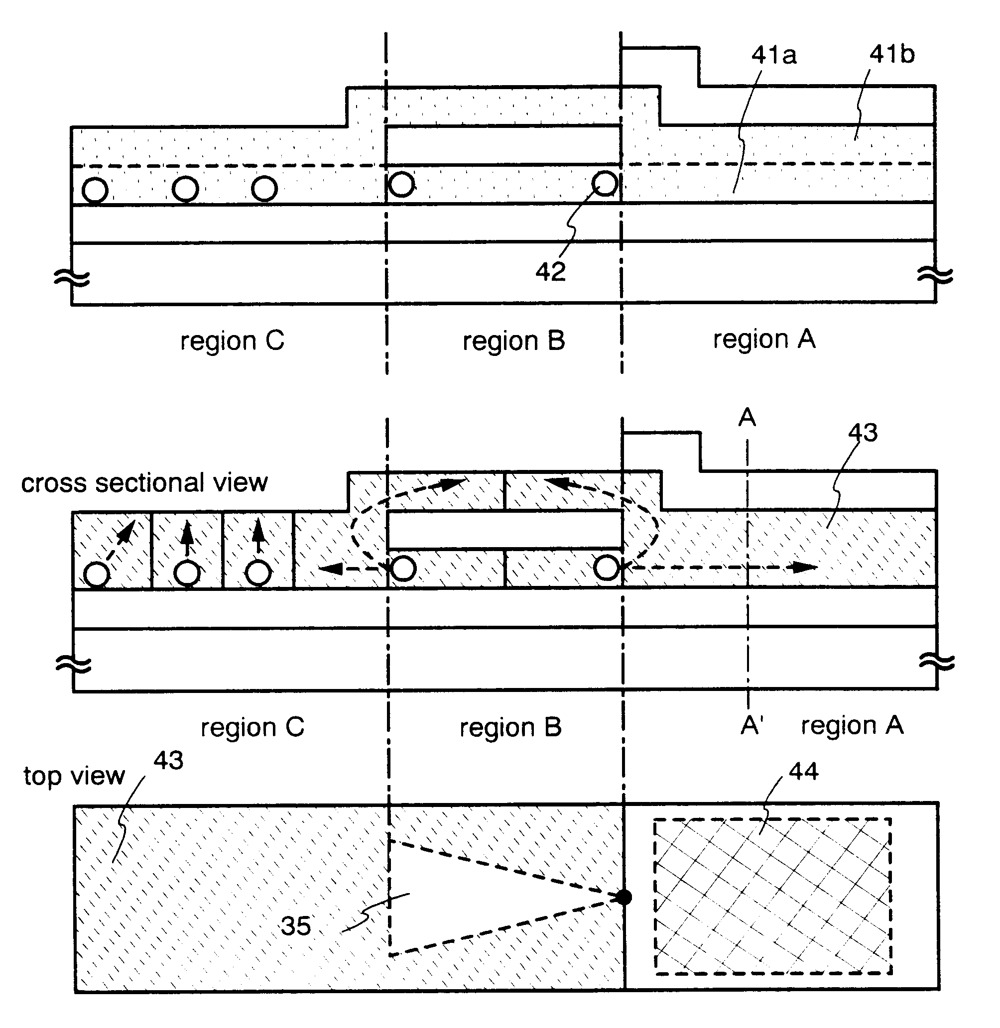
Embodiments of the present invention are explained using the cross sectional diagrams of FIGS. 3A to 4D. Note that a top surface diagram is also given along with a cross sectional diagram for FIGS. 3B and 4D.

A synthetic quartz glass substrate, non-alkaline substrate such as barium borosilicate glass or aluminum borosilicate glass, or a transparent film or PC (polycarbonate), PAr (polyallylate), PES (polyether sulfone), or PET (polyethylene terephthalate) may be used as the substrate 11 in FIG. 3A. For example, a glass such as Corning Corp. 7059 glass or 1737 glass can be suitably used.

The base insulating film 12 made from a film such as silicon nitride, silicon oxynitride, or silicon oxide is formed with a thickness of 10 to 200 nm (preferably from 10 to 100 nm) on the substrate 11 by a known method (LPCVD, plasma CVD, and the like). A silicon oxynitride film having a film thickness of 50 nm (composition ratios: Si=32%; O=27%; N=24%; H=17%) is formed in embodiment 1.

Th...

embodiment 2

[Embodiment 2]

A method of performing laser annealing after partially crystallizing a semiconductor film by heat treatment is explained using the cross sectional diagrams of FIGS. 6A to 7D. Note that a top surface diagram is also given along with a cross sectional diagram for FIGS. 6B and 7D.

A synthetic quartz glass substrate, non-alkaline glass substrate such as barium borosilicate glass or aluminum borosilicate glass, or a transparent film such as PC (polycarbonate), PAr (polyallylate), PES (polyether sulfone), or PET (polyethylene terephthalate) may be used as a substrate 31 in FIG. 6A. For example, a glass such as Coming Corp. 7059 glass or 1737 glass can be suitably used.

A base insulating film 32 made from a film such as silicon nitride, silicon oxynitride, or silicon oxide is formed with a thickness of 10 to 200 nm (preferably from 10 to 100 nm) on the substrate 31 by a known method (LPCVD, plasma CVD, and the like). A silicon oxynitride film having a film thickness of 50 nm (c...

embodiment 3

[Embodiment 3]

An embodiment of the present invention is explained using the cross sectional diagrams of FIGS. 8A to 9C. Note that a top surface diagram is also given along with a cross sectional diagram for FIGS. 8B and 9C.

A synthetic quartz glass substrate, non-alkaline glass substrate such as barium borosilicate glass or aluminum borosilicate glass, or a transparent film such as PC (polycarbonate), PAr (polyallylate), PES (polyether sulfone), or PET (polyethylene terephthalate) may be used as a substrate 51 in FIG. 8A. For example, a glass such as Corning Corp. 7059 glass or 1737 glass can be suitably used.

A base insulating film 52 made from a film such as silicon nitride, silicon oxynitride, or silicon oxide is formed with a thickness of 10 to 200 nm (preferable from 10 to 100 nm) on the substrate 51 by a known method (LPCVD, plasma CVD, and the like). A silicon oxynitride film having a film thickness of 50 nm (composition ratios: Si=32%; O=27%; N=24%; H=17%) is formed in embodim...


PUM

PropertyMeasurementUnit
angleaaaaaaaaaa
lengthaaaaaaaaaa
diameteraaaaaaaaaa

Abstract

A first insulating layer is embedded within a semiconductor film formed on a base insulating film, a second insulating layer is formed on a portion of the semiconductor film, and a laser beam is irradiated from the top side (or from both the top side and the bottom side) of the substrate. A thermal gradient develops in the semiconductor film due to the thermal insulating effect of the base insulating film, due to the thermal insulating effect of the first insulating layer, and due to the antireflection effect and thermal insulating effect of the second insulating layer. The location and direction of lateral growth of crystal nuclei are controlled by utilizing these effects, and large size crystal grains can be obtained.

Description

1. Field of the InventionThe present invention relates to a method of manufacturing a semiconductor device having a circuit constituted of a thin film transistor (hereafter referred to as a TFT). For example, the present invention relates to an electro-optical device, typically an EL display device or a light-emitting device, and to the structure of electronic equipment in which an electro-optical device is included as a part. Further, the present invention relates to a method of manufacturing the above device. Note that, throughout this specification, the category "semiconductor device" indicates general devices which can function by utilizing semiconductor characteristics, and the above electro-optical devices and electronic equipment are within the semiconductor device category.2. Description of the Related ArtResearch into techniques of increasing crystallinity when implementing laser annealing on an amorphous semiconductor film formed on an insulating substrate such as glass, t...

Claims


Application Information

Patent Timeline
Patent Type & Authority Patents(United States)
IPC IPC(8): H01L21/20H01L21/336H01L29/786H01L21/02H01L29/40H01L29/49H01L29/66
CPCH01L21/2026H01L29/4908H01L29/66757H01L29/78675H01L29/78684Y10S148/093H01L21/02488H01L21/02532H01L21/02686H01L21/02422
Inventor YOSHIMOTO, SATOSHI
Owner SEMICON ENERGY LAB CO LTD
Why Eureka
Try Eureka