Radiation-hardened silicon-on-insulator CMOS device, and method of making the same

a technology of silicon-on-insulator and cmos, which is applied in the direction of semiconductor devices, electrical equipment, transistors, etc., can solve the problems of radiation damage to the fabricated semiconductor structure, possible failure of any system incorporating,

Inactive Publication Date: 2003-03-11
PSEMI CORP
View PDF4 Cites 46 Cited by
  • Summary
  • Abstract
  • Description
  • Claims
  • Application Information

AI Technical Summary

Problems solved by technology

Semiconductor devices can be damaged or destroyed by the effects of ionizing radiation from natural and man-made sources.
Radiation changes the electrical properties of solid state devices, leading to possible failure of any system incorporating them.
For example, processing techniques such as reactive ion etching and plasma etching introduce some radiation damage into the fabricated semiconductor structure.
Both types of charges may or may not be produced in significant numbers as a result of the device being exposed to ionizing radiation.
While both conventional bulk CMOS devices and SOI CMOS devices may show degradation as a result of exposure to ionizing radiation, in SOI devices there are additional insulating layers (compared to bulk transistors) that can become charged as a result of radiation exposure.
This will result in current flow between the source and drain of the transistor, even without the presence of a gate bias.
This current is widely called "back channel" current to denote the fact that it is flowing near the back interface and is not capable of being controlled by the MOSFET gate.
Early attempts to fabricate this "ideal" silicon-on-insulator wafer were frustrated by a number of significant problems, which can be summarized as (1) substantial incursion of contaminants into the epitaxially deposited silicon layer, especially the p-dopant aluminum, as a consequence of the high temperatures used in the initial epitaxial silicon deposition and the subsequent annealing of the silicon layer to reduce defects therein; and (2) poor crystalline quality of the epitaxial silicon layers when the problematic high temperatures were avoided or worked around through various implanting, annealing, and / or regrowth schemes.
This effect represents a serious performance degradation for a MOS device; under normal conditions, MOS transistors are capable of offering a 10.sup.9 :1 ratio of on-state to off-state current.
In contrast to the ultrathin silicon-on-sapphire structures described above which are of high crystalline quality, these earlier SOS devices have relatively high defect levels in the silicon overlayers, a result of the lattice mismatch between the silicon and the insulating substrate.
While significant progress has been made in producing radiation-hardened MOS devices, these prior art techniques do not recognize or address the effects of the charging that occurs as a result of exposure to ionizing radiation, in the silicon-insulator interface region of the NMOS transistor formed in ultrathin silicon-on-sapphire.

Method used


Image

  • Radiation-hardened silicon-on-insulator CMOS device, and method of making the same
  • Radiation-hardened silicon-on-insulator CMOS device, and method of making the same
  • Radiation-hardened silicon-on-insulator CMOS device, and method of making the same

Examples


Embodiment Construction

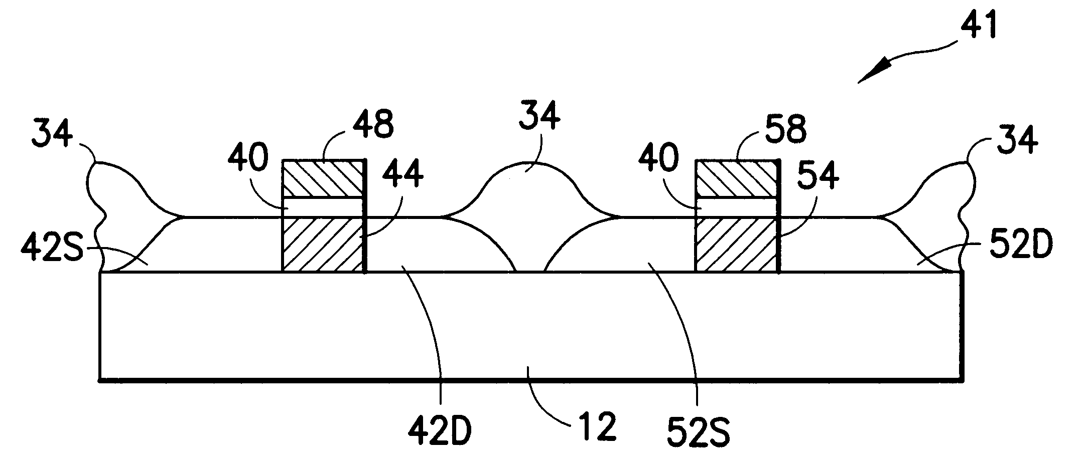
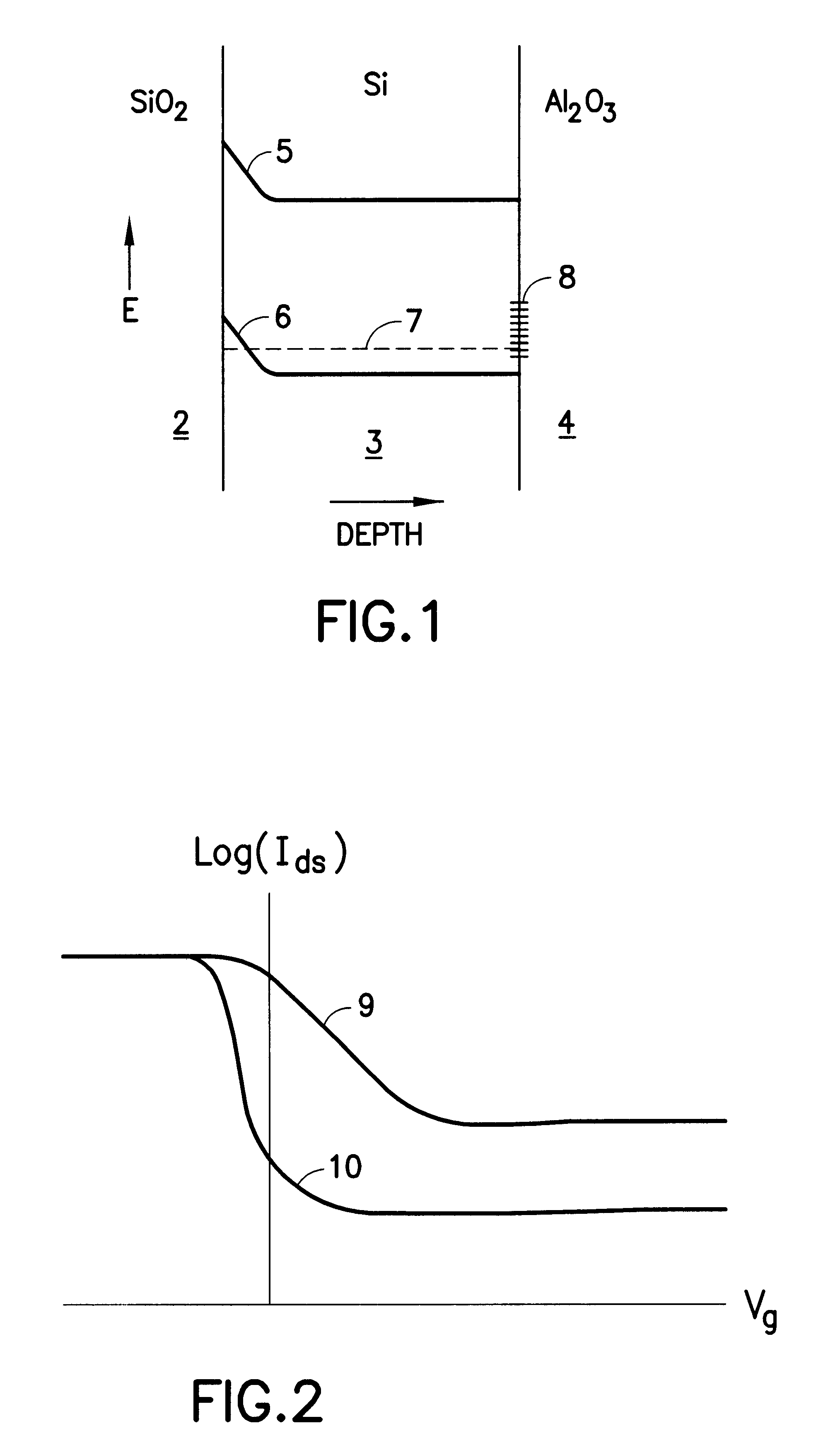
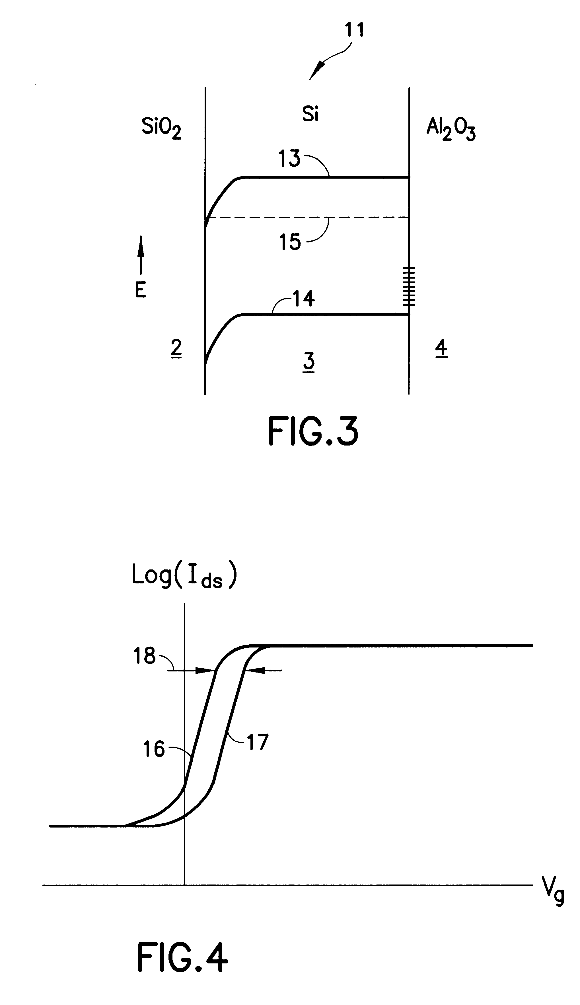
The invention is described in detail below with reference to the figures wherein like reference numerals refer to like elements or regions throughout. The P-channel MOS devices are formed in ultrathin silicon-on-sapphire wafers, prepared by methods disclosed in, for example, U.S. Pat. Nos. 5,416,04; 5,492,857; 5,572,040; 5,596,205; 5,600,169; 5,663,570; 5,861,336; 5,863,823; 5,883,396; 5,895,957; 5,920,233; 5,930,638; 5,973,363; 5,973,382; and 6,057,555.

To accomplish an effective radiation-hardening retrograde doping profile, the dopant concentration in the channel region can be controlled by well-known methods, e.g. ion implantation or epitaxy. Formation (by both ion implantation and epitaxy) and properties of semiconductors with retrograde doping profiles are discussed, for example, by Wolf (Silicon Processing for the VLSI Era. Volume 3: The Submicron MOSFET. Wolf, S.; Lattice Press, Sunset Beach, Calif., 1995; pages 539-555).

As used herein, the terms "retrograde doping profile" a...


PUM


Abstract

A method for eliminating the radiation-induced off-state current in the P-channel ultrathin silicon-on-sapphire transistor, by providing a retrograde dopant concentration profile that has the effect of moving the Fermi level at the back of the device away from that part of the bandgap where the interface states are located. When the Fermi level does not swing through this area in any region of operation of the device, subthreshold stretchout of the I-V curves does not occur.

Description

1. Field of the InventionThis invention generally relates to semiconductor devices and processes and more specifically to a method of fabricating and processing P-channel transistors in silicon layers formed on insulating substrates to obtain devices having high degrees of total dose radiation hardness.2. Description of Related ArtMetal oxide semiconductor (MOS) technology is virtually the standard for digital circuits used in computers and telecommunication devices today Increasingly, CMOS (complementary MOS) technology is utilized in these applications. CMOS technology incorporates both N-channel MOS and P-channel MOS transistors in the same monolithic structure."Radiation hardness" refers to the ability of a semiconductor device to withstand ionizing radiation without significant alteration of its electrical characteristics. A semiconductor device is said to be radiation hardened (rad-hard), radiation tolerant, or radiation resistant if it can continue to function within specific...

Claims


Application Information

Patent Timeline
Patent Type & Authority Patents(United States)
IPC IPC(8): H01L27/12H01L21/70H01L21/86
CPCH01L27/1203H01L21/86
Inventor CABLE, JAMES S.LYONS, EUGENE F.STUBER, MICHAEL A.BURGENER, MARK L.
Owner PSEMI CORP
Why Eureka
Try Eureka