
Diamond coatings on reactor wall and method of manufacturing thereof

a technology of diamond coating and reactor wall, which is applied in the field of semiconductor processing equipment, can solve the problems of corrosion of the components of such equipment, cracking of the coating, and a thickness below 5 .mu.m, and is stated to be unfavorabl

Inactive Publication Date: 2003-03-25
LAM RES CORP
View PDF41 Cites 112 Cited by
  • Summary
  • Abstract
  • Description
  • Claims
  • Application Information

AI Technical Summary

Benefits of technology

In view of the need for high purity and corrosion resistance for components of semiconductor processing equipment, there is a need in the art for improvements in materials and / or coatings used for such components. Moreover, with regard to the chamber materials, any materials which can increase the service life of a plasma reactor chamber and thus reduce the down time of the apparatus, would be beneficial in reducing the cost of processing the semiconductor wafers.

Problems solved by technology

The components of such equipment are subject to a variety of corrosive conditions associated with semiconductor processing.
The '013 patent states that the differences in thermal expansion coefficients between aluminum and ceramic coatings such as aluminum oxide leads to cracking of the coatings due to thermal cycling and eventual failure of the coatings in corrosive environments.
A thickness below 5 .mu.m, however, is stated to be unfavorable since the protection of the aluminum substrate is insufficient.

Method used


Image

  • Diamond coatings on reactor wall and method of manufacturing thereof
  • Diamond coatings on reactor wall and method of manufacturing thereof

Examples


Embodiment Construction

The invention provides an effective way to provide corrosion resistance to metal, ceramic and polymer surfaces of components of semiconductor processing apparatus such as parts of a plasma processing reactor chamber by utilizing an erosion resistant coating. Such components include chamber walls, substrate supports, gas distribution systems including showerheads, baffles, rings, nozzles, etc., fasteners, heating elements, plasma screens, liners, transport module components, such as robotic arms, fasteners, inner and outer chamber walls, etc., and the like.

Although the invention is applicable to any type of component having a metal, ceramic or polymer surface, for ease of illustration, the invention will be described in more detail with reference to the apparatus described in U.S. Pat. No. 5,820,723 which is incorporated herein by reference in its entirety.

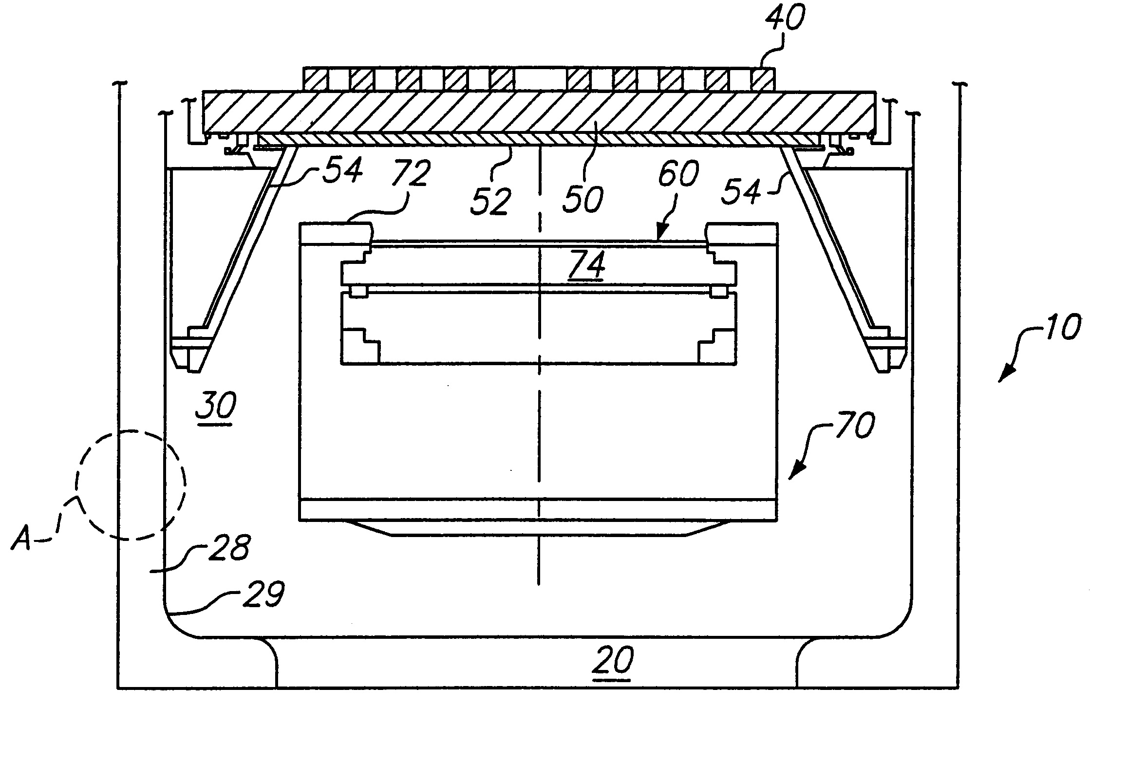
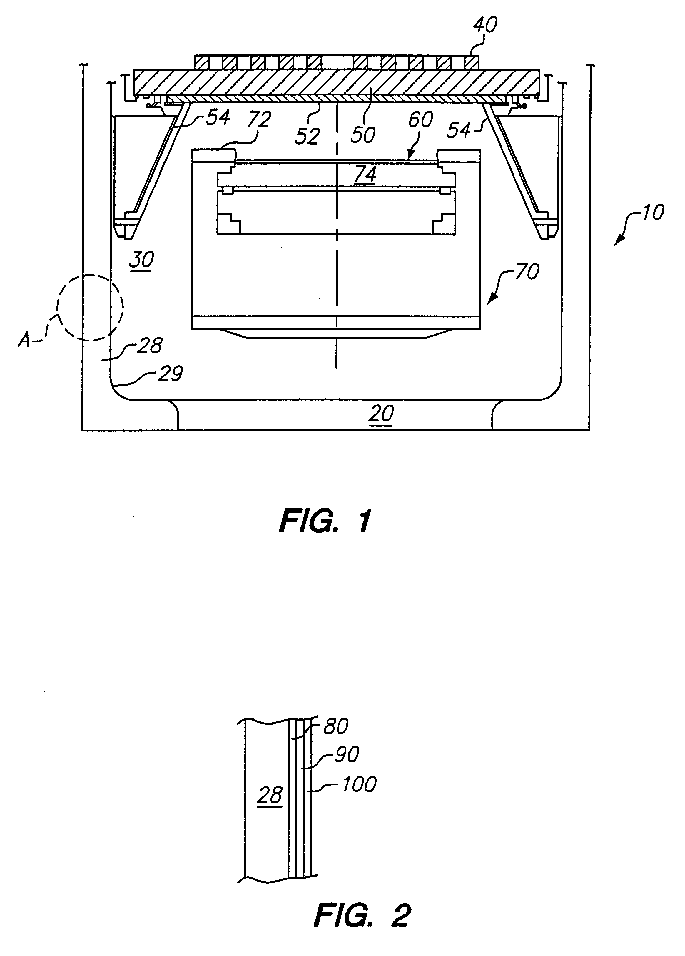
FIG. 1 illustrates a vacuum processing reactor chamber 10 that includes a substrate holder 70 providing an electrostatic clamping...


PUM

PropertyMeasurementUnit
thicknessaaaaaaaaaa
thicknessaaaaaaaaaa
thicknessaaaaaaaaaa

Abstract

A corrosion resistant component of semiconductor processing equipment such as a plasma chamber includes a diamond containing surface and process for manufacture thereof.

Description

1. Field of the InventionThe present invention relates to semiconductor processing equipment and a method of improving corrosion resistance of such components.2. Description of the Related ArtIn the field of semiconductor processing, vacuum processing chambers are generally used for etching and chemical vapor deposition (CVD) of materials on substrates by supplying an etching or deposition gas to the vacuum chamber and application of an RF field to the gas to energize the gas into a plasma state. Examples of parallel plate, transformer coupled plasma (TCP.TM.) which is also called inductively coupled plasma (ICP), and electron-cyclotron resonance (ECR) reactors and components thereof are disclosed in commonly owned U.S. Pat. Nos. 4,340,462; 4,948,458; 5,200,232 and 5,820,723. Because of the corrosive nature of the plasma environment in such reactors and the requirement for minimizing particle and / or heavy metal contamination, it is highly desirable for the components of such equipme...

Claims


Application Information

Patent Timeline
Patent Type & Authority Patents(United States)
IPC IPC(8): B01J19/02C23C16/26C23C16/02C23C16/27C23C16/44H01J37/32C23C14/06C23C30/00H01L21/205H01L21/3065
CPCB01J19/0073B01J19/02C23C16/27C23C16/4404H01J37/32495C23C16/0272B01J2219/0231B01J2219/025Y10T428/30Y10T428/26Y10T428/31678C23C16/44
Inventor O'DONNELL, ROBERT J.DAUGHERTY, JOHN E.CHANG, CHRISTOPHER C.
Owner LAM RES CORP
Learn More