Method and apparatus for linking and/or patterning self-assembled objects

a self-assembled object and method technology, applied in the field of methods and apparatus for linking and/or patterning self-assembled objects, can solve the problems of complex and expensive lithographic processes, end of scaling approach, loss of stored information,

Inactive Publication Date: 2003-05-20
GLOBALFOUNDRIES US INC
View PDF5 Cites 35 Cited by
  • Summary
  • Abstract
  • Description
  • Claims
  • Application Information

AI Technical Summary

Benefits of technology

As a second example, this invention may relate to fabrication of highly sensitive sensors [D. R. Baselt, et al, Proceedings of the IEEE, 85, 672 (1997); Q. Sqalli, M. P. Brenal, P. Hoffmann, F. Marquis-Weible, Appl. Phys. Lett. 76, 2134 (2000)]. Novel sensors, especially for near-field sensing, rely on a technique that can generate nanostructures preferably at the end of a sharp probe such as an atomic force microscope (U.S. Pat. No. 5,237,859) or a scanning tunneling microscope (U.S. Pat. No. 4,343,993) probe. More specifically, the present invention may allow to link a small magnetic nanoparticle (e.g. radius<10 nm) to the end of a, preferably heated, AFM / STM-probe, which results in high sensitivity for magnetic force sensing at high spatial resolution. Further, the present invention may be suitable to arrange a small highly polarizable nanoparticle at the end of a sharp probe (e.g., silicon probe or carbon nanotube), which can act as a small antenna greatly enhancing near-field optical sensing capabilities.
As a third example, this invention may relate to the preparation of efficient catalysts [A. S. Eppler et al., J. Phys. Chem. B, 104, 7286 (2000)]. Catalytic reactions generally require high pressure and high temperature conditions. However, current catalysts of small sized particles tend to aggregate under such conditions, resulting in the loss of their catalytic properties. This invention discloses a method and an apparatus, which avoids the aggregation of these particles, especially since the distance between the particles / islands of particles can be easily tuned.
The present invention builds upon the notion of self-assembly. Self-assembly is a low-cost and alternative (e.g., non-lithographic) way to organize objects, preferably nanoparticles, whereby these objects are used as functional building blocks for device fabrication, see U.S. Pat. No. 6,162,532, and U.S. patent application Ser. No. 09 / 359,638, now U.S. Pat. No. 6,254,662, both of which introduce the self-assembly of magnetic nanoparticles into magnetic nanoparticle superlattices, and are hereby incorporated by reference; and an article by S. Sun, C. B. Murray, D. Weller, L. Folks, and A. Moser, Science 287, 1989 (2000). The self-organization is influenced by the nature of the interactions exhibited among the stabilized particles. Generally, it relies on weaker and less directional interactions, such as van der Waals interactions, to organize the particles, and as a result, the assembly is not robust in its initial form. Thermal annealing has been applied to induce the transformation of organic stabilizers around each particle to polymer or inorganic matrix that can efficiently increase the robustness of the assemblies [S. Sun, C. B. Murray, D. Weller, L. Folks, A. Moser, Science, 287, 1989 (2000).].
With the invention, by applying an energy source locally to a specific area, the assembly in that area is hardened and can also adhere to the substrate well. The unirradiated self-organized nanoparticles, connected by weak interactions, can be easily washed away with a solvent as described in detail below, whereby self-assembled nanoparticle dot patterns are formed. With the invention, the height / thickness of the dots can be tuned all the way down to 2 nm via the self-assembly deposition technique, and the diameter (or lateral dimension) of the dots can be tuned down to less than 10 nm depending on the energy source used. Thermal annealing may be applied to the patterned dots to control their physical properties as well. The reported procedure does not need prior substrate modification, as in common lithographic processes, and allows for patterning on any size and shaped substrates. In summary, this invention offers a low cost solution to patterned media by providing controlled assemblies of dot arrays over larger areas, and allowing for patterning with high lateral resolution.

Problems solved by technology

However, this scaling approach will come to an end in the near future, because with decreasing grain size the thermal energy can reverse more easily the magnetization direction (superparamagnetism), which eventually will result in the loss of the stored information.
Previous efforts in fabricating such dot arrays relied on complicated and expensive lithographic processes, including e-beam lithography [R. M. H. New, R. F. W. Pease, R. L. White, J. Vac. Sci. Technol.
However, good control of nanoparticle-containing dots has not been reached.
Catalytic reactions generally require high pressure and high temperature conditions.
However, current catalysts of small sized particles tend to aggregate under such conditions, resulting in the loss of their catalytic properties.
Generally, it relies on weaker and less directional interactions, such as van der Waals interactions, to organize the particles, and as a result, the assembly is not robust in its initial form.

Method used


Image

  • Method and apparatus for linking and/or patterning self-assembled objects
  • Method and apparatus for linking and/or patterning self-assembled objects
  • Method and apparatus for linking and/or patterning self-assembled objects

Examples


Embodiment Construction

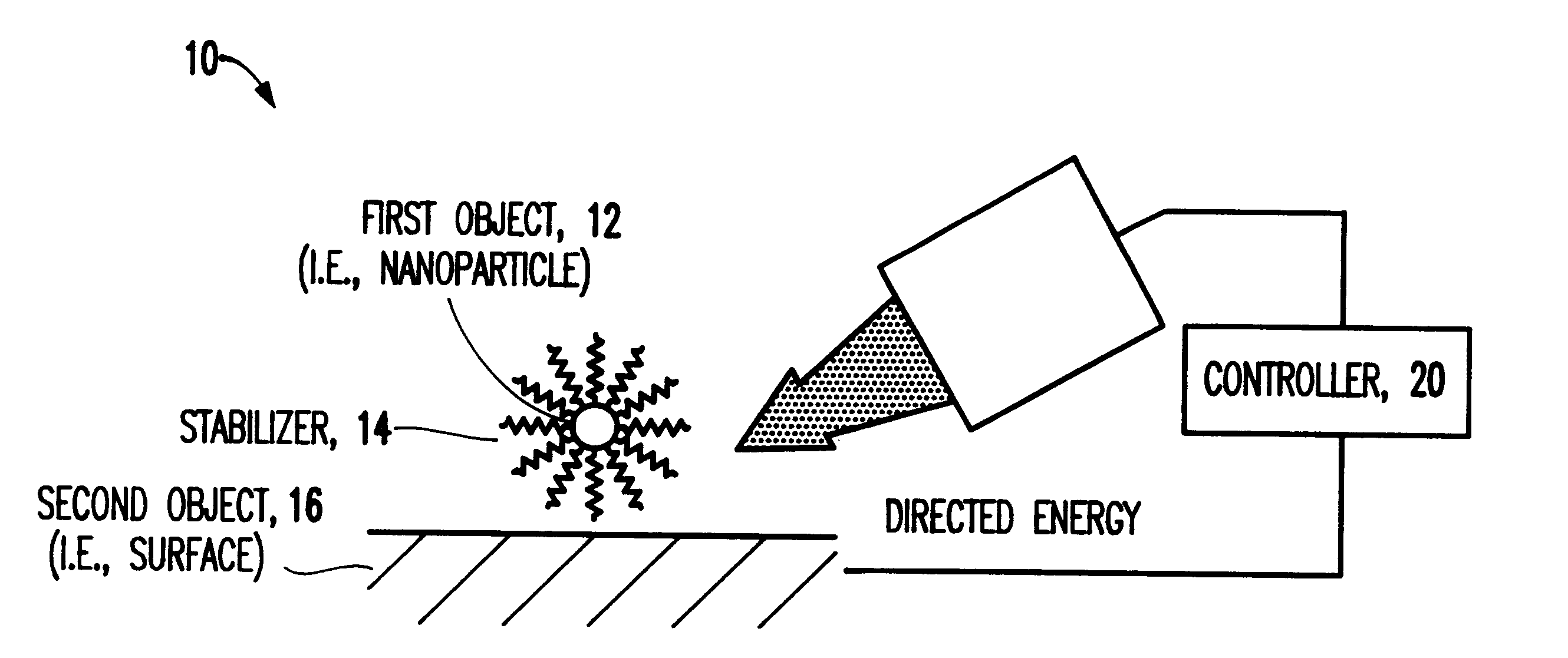
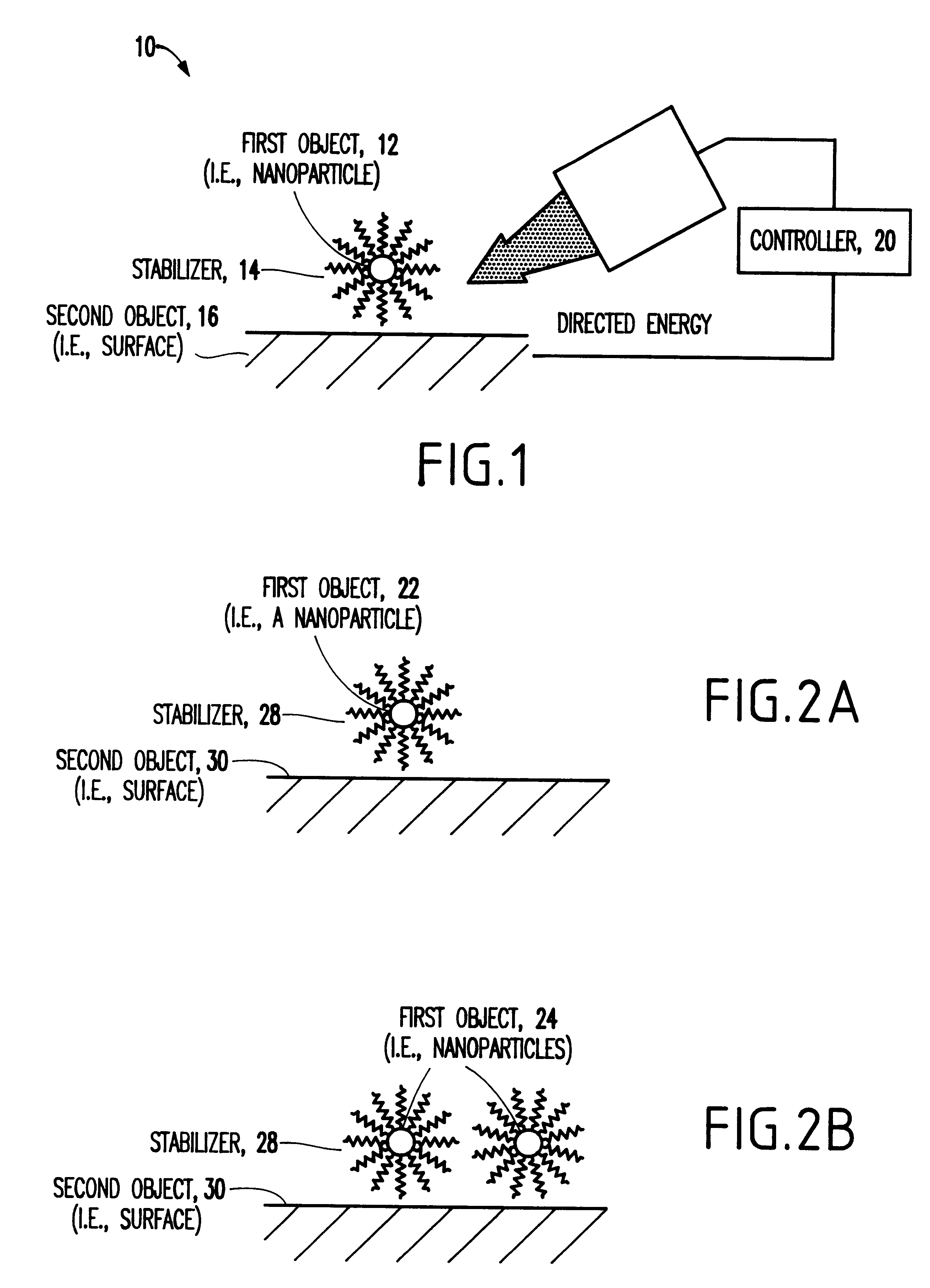
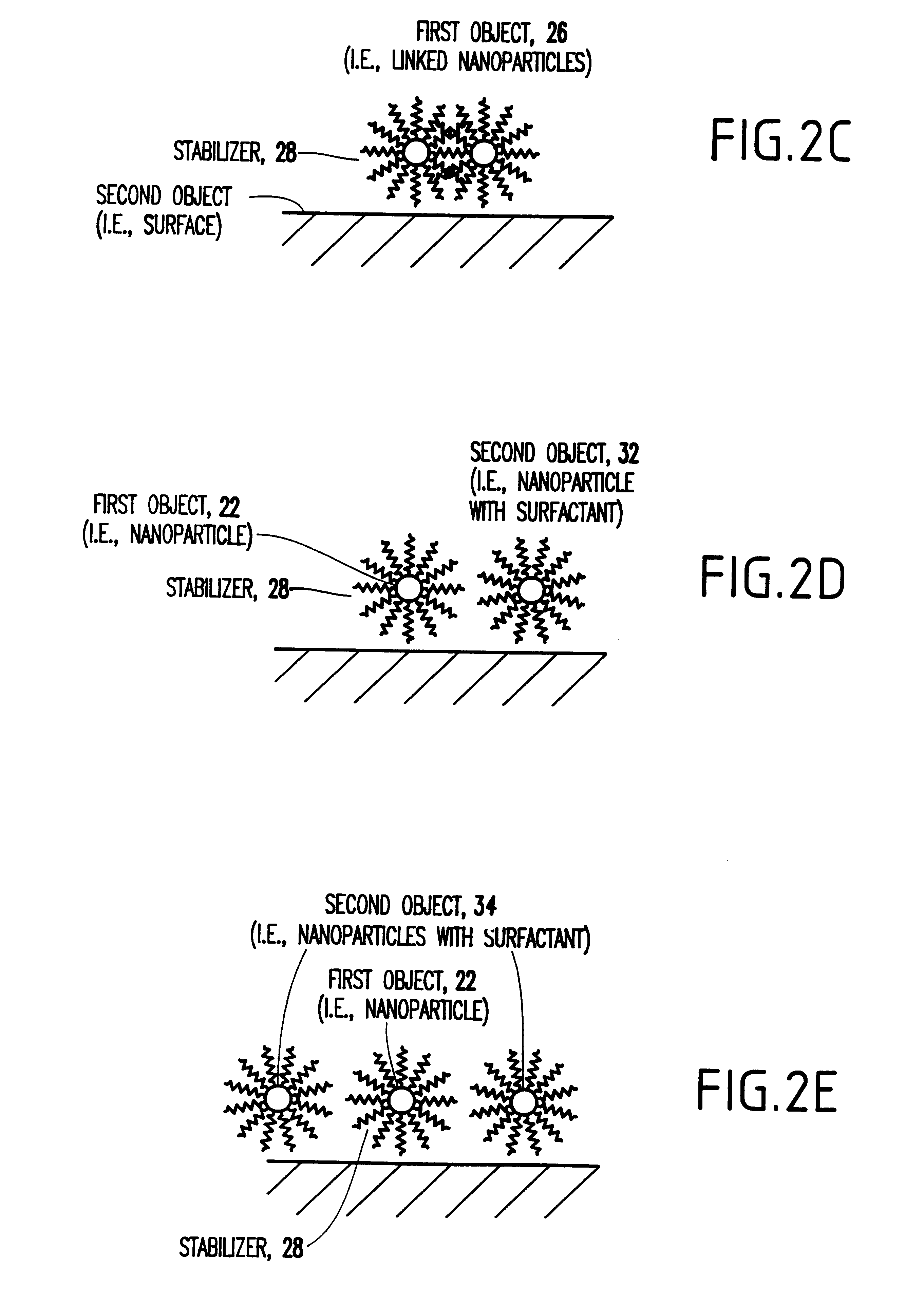
The present invention provides a method and an apparatus for linking and / or patterning self-assembled object(s). The method comprises materials that contain a first object with a stabilizer and a second object that can be linked to the first object. Energy is directed at the stabilizer to link the first and second objects. Finally, a solvent may be applied to the first and second objects to remove non-linked objects. As an example, the first object can comprise a FePt nanoparticle. Such a material is susceptible to linkage, and it displays potentially useful magnetic phase changes. When the energy is directed simultaneously at this nanoparticle and at the second object (another FePt nanoparticle or substrate) and at the stablizer that separates them, linkage of the objects is made. Applying this procedure to many such objects results in FePt nanoparticles being linked over a larger area.

FIG. 1 shows a generalized apparatus (10) in accordance with the invention. In particular, the ap...


PUM

PropertyMeasurementUnit
sizeaaaaaaaaaa
diameteraaaaaaaaaa
height/thicknessaaaaaaaaaa

Abstract

The invention provides a method and related apparatus to link and / or pattern self-assembled first objects to a second object. Each of the first object (e.g., a nanoparticle) can be embedded in a mobile binder (i.e., a stabilizer). The invention applies energy to the first object and stabilizer, links this first object to the second object, and provides a controlled linkage of the first object with respect to the second object. Applying this procedure to many such objects results in a larger areal arrangement of these linked objects. An appropriate solvent may be used to remove non-linked objects, yielding a patterned array. Thermal annealing can be applied to control the physical and chemical properties of the array.

Description

The present invention generally relates to a method and an apparatus for controlled linking / patterning of self-assembled, preferably nano-sized objects, and more particularly to ultra-high density data storage.DESCRIPTION OF THE RELATED ARTThis invention can be applied to various technologies, which realization relies on a method and an apparatus for controlled linking / patterning of self-assembled objects. As a particular example, patterning self-assembled magnetic objects into object-containing dot arrays with precise control of dot size and inter-dot spacing has technologically great potential in future ultrahigh density magnetic data storage. Specifically, ultrahigh density magnetic storage requires continued down scaling of each individual storage bit. In the past, this growth of storage densities has been accomplished simply by scaling down the grain size in the magnetic media, while maintaining the numbers of grains constant within one bit cell due to signal to noise requireme...

Claims


Application Information

Patent Timeline
Patent Type & Authority Patents(United States)
IPC IPC(8): G03F7/038G03F7/16G11B5/855
CPCB82Y30/00G03F7/038G03F7/165Y10S977/901G11B5/855
Inventor BAGLIN, JOHN E. E.HAMANN, HENDRIK F.SUN, SHOUHENG
Owner GLOBALFOUNDRIES US INC
Why Eureka
Try Eureka