

Device for gas sensing
- Summary
- Abstract
- Description
- Claims
- Application Information
AI Technical Summary
Benefits of technology
Problems solved by technology
Method used
Image

Examples
example 1
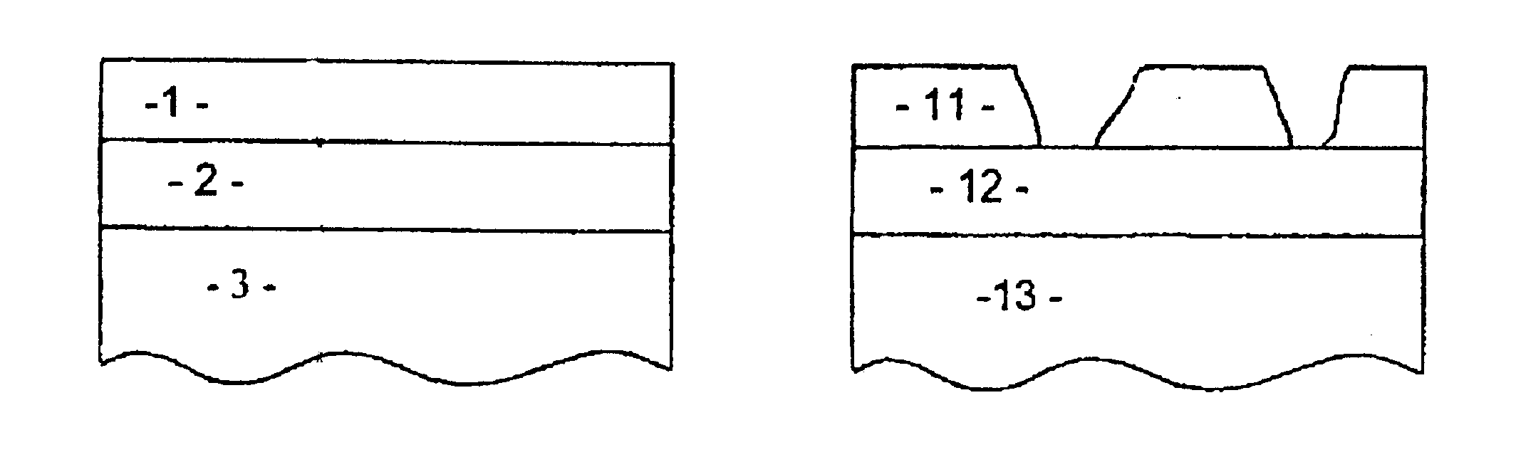
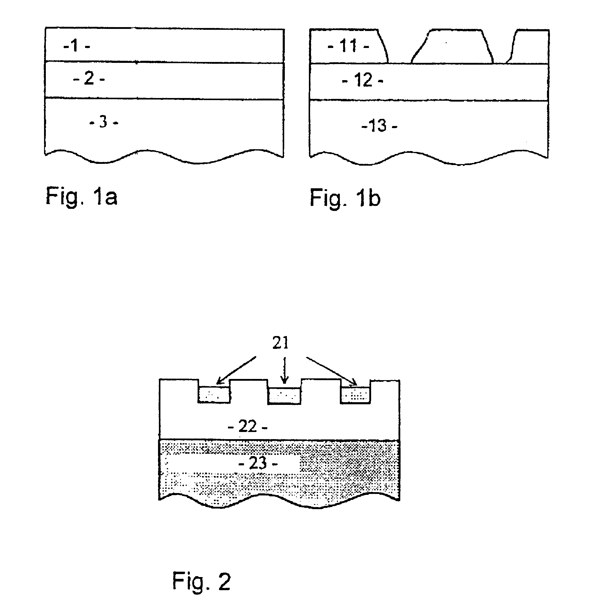
Above, it is mentioned that a semiconducting substrate or insulating layer with suitable morphology can be obtained using masking, lithography, and etching techniques. This process could, e.g., consist of the following steps. A resist is deposited onto the material that should be given a suitable morphology. The resist is patterned using e-beam lithography, e.g., by exposing a pattern of squares or circles of a suitable size, typically 100-10000 .ANG.. After development of the resist, the unexposed resist is removed and the material below is etched to a suitable depth, typically 100-1000 .ANG.. The resulting surface will consist of a regular array of 100-1000 .ANG. high protrusions separated by trenches. The trenches will all be interconnected and the protrusions will be covered by resist.
(a) If the above described masking, lithography, and etching process is performed using a semiconducting substrate, a field-effect gas sensor according to the above described first object of the in...
example 2
Above, it is mentioned that a semiconducting substrate or insulating layer with suitable morphology can be obtained by utilising a naturally obtained morphology resulting from, e.g., an etching process or a deposition technique. Examples of etching techniques are the well-known (photo)electrochemical fabrication of porous layers of silicon and silicon carbide. The resulting layers do not have the extremely regular morphology as that which can be obtained using masking, lithography, and etching techniques, but the average morphology can be controlled to a high degree of accuracy. Although it is possible to prepare highly porous layers using (photo)electrochemical etching processes, it is sufficient for the purpose of this invention to prepare layers with a roughness on a scale of typically 100-1000 .ANG.. Once these rough layers have been prepared, functioning field-effect gas sensor devices according to objects 2, 4, and 6 of this invention can be fabricated in analogy to the exampl...
example 3
Above, it is mentioned that a semiconducting substrate or insulating layer with suitable morphology can be obtained by utilising a naturally obtained morphology resulting from, e.g., an etching process or a deposition technique. An example of a deposition technique is the previously known deposition of cerium dioxide films. It has been shown that it is possible to grow cerium dioxide with preferentially exposed (111) surfaces in pyramidal protrusions on top amorphous silicon dioxide. The pyramidal protrusions typically have a lateral size of 100-800 .ANG. and a height of 50-250 .ANG.. Functioning field-effect gas sensor devices according to object 6 of this invention can be fabricated using these naturally microstructured cerium dioxide films in analogy to the example 1(d) above. This particular example is especially interesting in view of the known catalytic properties of cerium dioxide, which can be modified e.g. by adding trace amounts of copper such that a wide range of differen...
PUM
 Abstract
Description
Claims
Application Information